

RFIC design is the branch of RF design that builds radio-frequency circuits such as LNAs, mixers, oscillators, PLLs and power amplifiers as integrated circuits on a semiconductor die, usually in CMOS or SiGe BiCMOS, rather than from discrete parts on a board. It trades the freedom of discrete components for integration, low cost in volume and close coupling with digital logic.
Almost every phone, Wi-Fi access point, Bluetooth device, GNSS receiver and automotive radar sensor relies on one or more RFICs. This introduction explains the processes they are built in, the passive components available on chip, the design flow from specification to silicon, and how RFIC work differs from board-level and MMIC design. It is the RFIC section of the RF design guide, and it builds on the RF fundamentals, transmission line and S-parameter sections.
What Is RFIC Design?
An RFIC designer works with the same specifications as a board-level designer: gain, noise figure, linearity, phase noise, output power and efficiency. The difference is in the materials. Every transistor, inductor and capacitor is drawn in a layout tool and fabricated in a foundry process, so the designer chooses device sizes and geometry rather than part numbers. Off-chip components are reduced to those that cannot be integrated well: high-Q filters, crystals, antennas and, in many products, the final power amplifier.
That freedom comes with constraints. Silicon substrates are conductive and lossy, supply voltages are low, on-chip inductors have modest Q, and a mistake costs a fabrication cycle of weeks to months. Good RFIC design is therefore heavily simulation-driven, with careful modelling of layout parasitics before tape-out. An earlier overview on the site, what is RF integrated circuit design, gives additional background.
CMOS and SiGe Processes
Most RFICs are built in one of three silicon process families. The RF transistor technologies page compares their device-level figures of merit with GaAs and GaN.
- Bulk CMOS: the default for highly integrated transceivers. Fine-geometry nodes give transistors with fT in the hundreds of gigahertz, and the RF circuitry shares the die with digital baseband, data converters and control. The costs are low supply voltage, which limits output power and dynamic range, and a lossy substrate.
- SOI CMOS: CMOS on an insulating buried oxide. Lower parasitic capacitance and better isolation make it the standard process for RF switches and tuners, and it allows transistors to be stacked to handle higher voltages.
- SiGe BiCMOS: adds silicon-germanium heterojunction bipolar transistors to a CMOS process. The HBTs offer high fT and fmax, good matching, higher breakdown than fine-node CMOS and low 1/f noise. That suits VCOs, mmWave front ends and automotive radar chips.
A foundry supplies the process design kit (PDK): device models, layout rules, parameterised cells for transistors and passives, and verification decks. The accuracy of the PDK models, especially for inductors and transistors at high frequency, largely determines how close first silicon comes to simulation.
What an RFIC Integrates
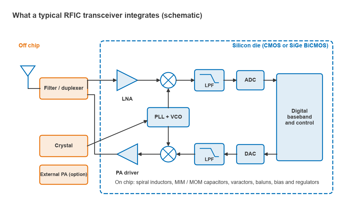
A typical single-chip transceiver contains the LNA, down-conversion mixers, baseband filters and ADCs on the receive side, DACs, filters, up-conversion mixers and a PA driver on the transmit side, and a shared PLL and VCO. The digital baseband and control logic often sit on the same die. Architectures that suit integration, such as zero-IF and low-IF receivers, dominate because they avoid off-chip IF filters. The filter or duplexer, the crystal reference and often an external PA remain off chip.
On-Chip Passives
Passive components are often the hardest part of an RFIC, because they occupy most of the area and set the losses.
- Spiral inductors: drawn in the thick top metal layers. Their Q is limited by metal resistance, skin and proximity effects, and eddy currents and capacitance to the substrate. Typical values fall in the range of about 10 to 20 at a few gigahertz, far below discrete chip inductors. Patterned ground shields and thick metal help.
- Capacitors: metal-insulator-metal (MIM) and metal-oxide-metal (MOM) capacitors offer good linearity and Q; MOS capacitors offer high density but depend on voltage.
- Varactors: accumulation-mode MOS varactors tune VCOs, as described in VCO design.
- Transformers and baluns: coupled spirals that provide impedance transformation, DC isolation and single-ended to differential conversion. See RF baluns.
- Transmission lines: at mmWave, wavelengths are short enough that microstrip and coplanar lines on chip become practical matching elements, as discussed in mmWave radio architectures.
Worked example: a spiral inductor and an LC load
A first estimate of spiral inductance comes from the modified Wheeler formula, L = K1μ0n2davg/(1 + K2ρ), where for a square spiral K1 = 2.34 and K2 = 2.75, davg is the mean of the outer and inner diameters and ρ = (dout − din)/(dout + din) is the fill ratio. For n = 3 turns, dout = 200 µm and din = 100 µm, davg = 150 µm and ρ = 0.333, giving L = 2.07 nH.
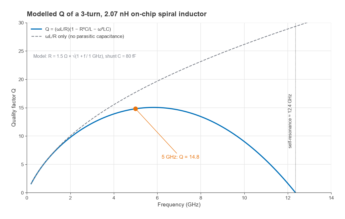
Assume the series resistance rises with frequency as R = 1.5 Ω × √(1 + f/1 GHz), which is 3.67 Ω at 5 GHz, and the inductor has 80 fF of parasitic capacitance. Then ωL = 65.1 Ω and the simple quality factor ωL/R is 17.7. Including the capacitance with Q = (ωL/R)(1 − R2C/L − ω2LC) reduces it to 14.8, and the inductor self-resonates at about 12.4 GHz. These model values are illustrative; in a real design they come from the PDK or from EM simulation.
Used as the load of a tuned amplifier at 5 GHz, the inductor needs 0.489 pF of total capacitance to resonate. The equivalent parallel resistance of the tank is Rp ≈ Q·ωL = 963 Ω, so a transistor with gm = 20 mS gives a voltage gain of gmRp = 19.3, or 25.7 dB. The inductor Q directly sets gain, and in an oscillator it sets phase noise, which is why so much RFIC effort goes into passives. The Q factor page covers the general relationships.
The RFIC Design Flow
A typical flow runs as follows.
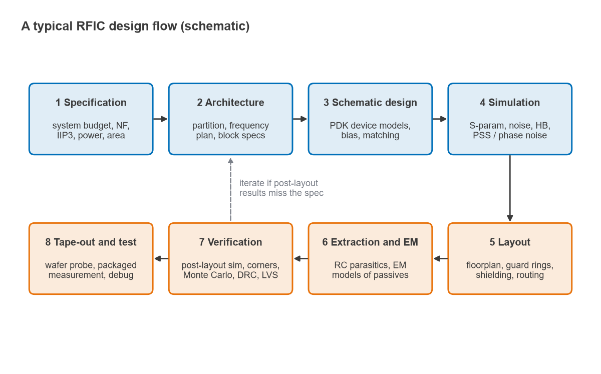
- Specification and architecture: a system budget assigns gain, noise figure, IIP3, phase noise and power consumption to each block, and the frequency plan is fixed.
- Schematic design and simulation: circuits are designed with PDK models and simulated with S-parameter, noise and transient analyses, plus harmonic balance or periodic steady-state analysis for mixers, oscillators and PAs.
- Layout: devices and passives are placed with attention to symmetry, guard rings, substrate contacts, supply routing and isolation between noisy and sensitive blocks.
- Extraction and EM modelling: parasitic resistance and capacitance are extracted, and inductors, transformers and critical interconnect are modelled with EM simulation.
- Verification: post-layout simulation over process, voltage and temperature corners and Monte Carlo variation, with design rule and layout-versus-schematic checks.
- Tape-out and test: wafers are fabricated, then measured on a probe station or in packages and compared with simulation.
RFIC vs MMIC
An MMIC (monolithic microwave integrated circuit) is also an integrated RF circuit, but the term usually refers to compound-semiconductor chips in GaAs, GaN or InP on semi-insulating substrates. MMICs have better passive Q and higher breakdown, so they excel at power amplifiers, LNAs and switches at microwave and mmWave frequencies, but they integrate little or no digital logic. RFICs in silicon integrate whole transceivers at low cost in volume. Many products use both, for example a silicon transceiver driving a GaAs or GaN front-end module. The MMIC vs RFIC vs discrete design page compares the three approaches in detail.
Frequently Asked Questions
What is RFIC design?
It is the design of radio-frequency circuits as integrated circuits, usually in CMOS or SiGe BiCMOS. It covers transistor-level design of LNAs, mixers, oscillators, PLLs and PAs, the on-chip passives they need, and the layout and verification required before fabrication.
RFIC vs MMIC: what is the difference?
RFICs are usually silicon chips that integrate RF, analog and digital functions at high volume. MMICs are usually GaAs, GaN or InP chips focused on microwave performance, such as high power, low noise or high frequency, with little digital content.
Why is the Q of on-chip inductors low?
Thin metal layers have significant resistance, which rises further with skin and proximity effects, and the conductive silicon substrate adds eddy-current loss and parasitic capacitance. Typical values are roughly 10 to 20 at a few gigahertz.
What should I learn before RFIC design?
Analog IC design, transistor small-signal models, noise and linearity theory, and RF fundamentals such as matching and S-parameters. The RF design learning roadmap and the best RF design books list suggest an order.
Related Topics
Continue with MMIC vs RFIC vs discrete design, the RF front-end modules part of the Radio Architectures series, PLL frequency synthesis and the low-noise amplifier design article.