

RF PCB layout is the part of printed circuit board design that treats every trace, via and ground connection as part of the circuit, because at radio frequencies their inductance, capacitance and length change gain, matching and isolation. To lay out an RF PCB, route RF signals as short controlled-impedance lines over an unbroken ground plane, ground every shunt part through its own vias, fence the RF path with stitching vias, and keep digital and switching circuits away from it.
Most layout problems at RF come down to one idea: current always returns along the path of lowest impedance, and at high frequency that path lies directly under the signal trace. Anything that interrupts or lengthens that return path adds inductance, radiates, or couples into a neighbour. The guidelines below follow from that. The sections link to the detailed pages in this cluster, which sits under the RF design pillar.
Step-by-Step Layout Procedure
- Choose the stackup first, with a solid ground layer directly under the RF layer and a dielectric thin enough to give practical 50 Ω trace widths.
- Place the RF parts in signal-flow order, from antenna to transceiver, so that RF lines are as short as possible and never cross each other.
- Calculate trace widths for the target impedance with the fabricator’s stackup data, and route RF lines with smooth or mitred bends.
- Ground every shunt component with at least one via placed at its pad, and use two or more where the part carries significant RF current.
- Fill unused areas on the RF layer with ground and stitch it to the ground plane, with a via fence along RF lines at a pitch well below a tenth of a wavelength.
- Keep clocks, digital buses and switching regulators physically away from the RF section, and decouple each RF supply pin locally.
- Leave room for a shield can, test points and a matching network footprint ahead of the antenna.
- Review the layout against the return-current path for every RF net, then simulate the critical sections with an EM solver if margins are tight.
Continuous Ground Plane Under RF Traces
A microstrip line is a two-conductor structure: the trace and the plane below it. The characteristic impedance, the field shape and the return current all depend on that plane being continuous. When a trace crosses a gap, split or slot in the plane, the return current has to detour around it. The detour adds series inductance, creates a slot that can radiate, and couples the RF signal into whatever else shares the disturbed region.
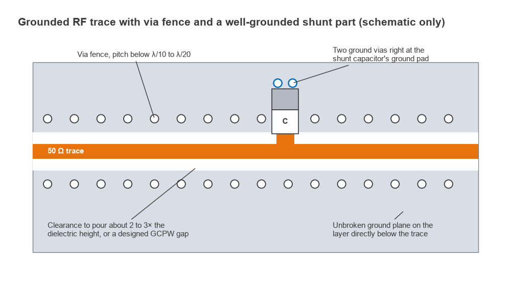
In practice this means:
- Dedicate the layer directly beneath the RF layer to ground, with no other signals routed on it in the RF area.
- Do not split the ground into separate “analog” and “digital” planes under or near RF traces. Partition by placement instead, and keep one plane.
- Avoid rows of closely spaced vias or clearance holes that perforate the plane under an RF line.
- Where an RF line must change layers, place a ground via beside each signal via so the return current can change reference planes at the same point.
The ground plane also sets the trace width. Using the Hammerstad microstrip equations with a dielectric constant of 4.3, a 50 Ω line over a 0.2 mm dielectric is about 0.39 mm wide, while the same line over a 1.6 mm two-layer board is about 3.1 mm wide, wider than most RF IC pads. That is the main reason RF boards use four or more layers with ground on layer 2. Material choice and stackups are covered in detail in FR-4 vs Rogers, and line calculations in the microstrip calculator.
Ground Vias and Via Stitching
A via is a short inductor. A widely used approximation for a via of length h and diameter d, both in millimetres, is
L ≈ 0.2h [ln(4h/d) + 1] nH
Worked example: via inductance at 2.4 GHz
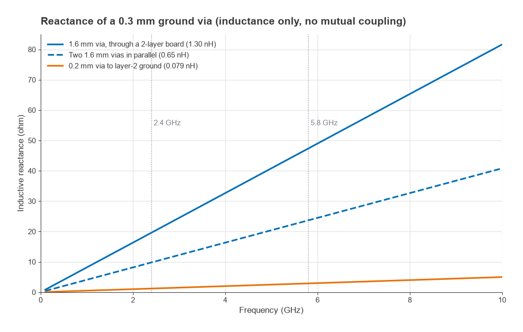
- A 0.3 mm via through a 1.6 mm board: L ≈ 0.2 × 1.6 × [ln(21.3) + 1] = 1.30 nH. At 2.4 GHz its reactance is 2π × 2.4 × 109 × 1.30 × 10−9 = 19.6 Ω, and at 5.8 GHz it is 47.3 Ω.
- A 0.3 mm via to a ground plane 0.2 mm below: L ≈ 0.2 × 0.2 × [ln(2.67) + 1] = 0.079 nH, or 1.19 Ω at 2.4 GHz.
Nearly 20 Ω in series with a shunt capacitor or a ground pin is a large fraction of a 50 Ω system. A shunt capacitor intended as an RF short is no longer a short, and an amplifier with an emitter or source lead grounded this way loses gain and may become unstable. Two vias in parallel roughly halve the inductance if they are spaced apart; vias placed very close together share flux and give less improvement.
Shunt component grounding
Place the ground via inside or immediately next to the ground pad of every shunt part, not at the end of a trace. Use two or more vias for shunt capacitors in matching networks, filter shunt elements, and the ground pads of amplifiers and RF ICs; exposed paddles normally need an array of vias. Do not share one via between several shunt parts in a filter, because the shared inductance couples their currents and fills in the stopband. The same reasoning applies to decoupling capacitors: a 100 pF capacitor with 0.5 nH of package inductance resonates near 661 MHz with a 0.079 nH via, but near 375 MHz with a 1.30 nH via.
Via fence and stitching spacing
Ground pour on the RF layer is only useful if it is tied to the plane below at short intervals. Otherwise sections of pour act as resonant patches or slot antennas. Published guidance on stitching pitch varies: λ/8, λ/10 and λ/20 are all quoted, and some designers use λ/20 for fences beside RF lines and λ/10 for general stitching. Here λ is the wavelength in the dielectric at the highest frequency of concern, including harmonics that must be contained.
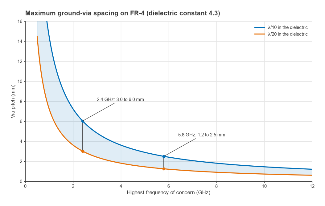
Using the bulk dielectric constant, which gives a slightly conservative result, λ = c / (f√εr). On FR-4 with εr = 4.3 at 2.4 GHz, λ = 60.3 mm, so λ/10 is 6.0 mm and λ/20 is 3.0 mm. At 5.8 GHz, λ = 24.9 mm and the pitch falls to 2.5 mm and 1.25 mm. A pitch of 2 to 3 mm is therefore a reasonable default for 2.4 GHz designs with some margin for harmonics. The detailed treatment is in RF grounding and via stitching.
Ground pour next to RF traces
Ground pour beside an RF trace improves isolation, but only if the impedance calculation accounts for it. Two approaches work. Either keep the pour far enough away that the line behaves as plain microstrip, typically a gap of at least two to three times the dielectric height, or design the line deliberately as grounded coplanar waveguide, with the gap included in the calculation. What causes trouble is pour placed at an arbitrary small gap, which lowers the impedance by an amount nobody calculated.
Short, Controlled-Impedance RF Lines
Every millimetre of line adds loss and phase shift, and every discontinuity adds a small reflection. Keep RF lines short and direct, and route them on the outer layer next to the ground reference.
- Controlled impedance. Specify the impedance and stackup to the fabricator and ask for a test coupon if the tolerance matters. Etching and dielectric tolerance commonly move impedance by several percent.
- Bends. A square 90° corner adds excess capacitance at the outer corner. At a few gigahertz the effect is small, but it is easy to avoid with a mitred corner or a curved bend with a radius of at least about three trace widths.
- Pad transitions. Component pads are usually wider than the line. Where the difference is large, cut out the ground under the pad on the layer below to keep the impedance close to 50 Ω, or accept the discontinuity and compensate in the matching network.
- Stubs. Avoid unused branches, test-point stubs and via stubs on RF lines; at a quarter wavelength a stub becomes a short.
Return loss and the effect of small mismatches are quantified in VSWR and return loss, and the underlying line theory is in transmission line theory.
Separating RF From Digital and Switching Circuits
Digital edges and switch-mode regulators produce harmonics that fall across the RF bands. A 26 MHz clock has harmonics at every multiple, including channels inside the 2.4 GHz band, and a switching regulator’s fast edges radiate from its switch node and input loop. Once that energy reaches the receiver input, no amount of filtering after the LNA removes it. The practical measures are:
- Place the RF section, digital section and power conversion in separate regions of the board, with the RF section at one edge near the antenna.
- Never route digital or clock lines under or beside RF traces, and avoid running them under the RF section on inner layers.
- Keep the hot loop of each switching regulator small and away from the RF area. Feed RF supplies through ferrite beads or LC filters and, where noise matters, a low-noise linear regulator.
- Decouple each RF supply pin with a small capacitor at the pin and a larger one nearby, each with its own ground via.
- Use a shield can over the RF section where the product needs it. See RF shielding, and for multi-radio products, coexistence and desense.
The same measures help a product pass radiated emissions testing, which is covered in EMC and EMI for RF designers.
Pages in This Section
- RF PCB materials and stackups: FR-4 vs Rogers: dielectric constant, loss and hybrid stackups.
- Grounding, via stitching and return paths: via inductance, fences and plane design.
- RF shielding cans and isolation: when a can is needed and how to lay one out.
- Power supply decoupling for RF circuits: capacitor resonance, ferrites and regulator noise.
- EMC and EMI for RF designers: emissions, immunity and their layout causes.
- Coexistence and desense in multi-radio products: keeping one radio from blinding another.
Frequently asked questions
How do you lay out an RF PCB?
Start with a stackup that puts a solid ground plane directly under the RF layer. Place parts in signal-flow order, route short controlled-impedance lines, ground each shunt part with its own vias, stitch ground pour with a via fence, and keep digital and switching circuits in a separate area.
How far apart should ground vias be?
Sources quote anything from λ/8 to λ/20, where λ is the wavelength in the board dielectric at the highest frequency of concern. On FR-4 at 2.4 GHz that is roughly 3 to 6 mm between λ/20 and λ/10. Use the tighter figure beside RF lines and in areas that must contain harmonics.
Should RF traces have ground pour next to them?
Yes, if it is stitched and either kept well clear of the trace or included in the impedance calculation as grounded coplanar waveguide. Unstitched pour, or pour at an uncalculated small gap, causes more problems than it solves.
Do right-angle bends matter at RF?
Below a few gigahertz the effect of a single square corner on a narrow trace is usually small. It grows with frequency and trace width, and mitred or curved bends cost nothing, so they are standard practice on RF lines.
Related topics
Layout interacts with almost every other part of a radio: S-parameters describe what a layout section does to the signal, impedance matching networks have to be laid out with the parasitics in mind, and PCB antenna design depends on the ground plane around the antenna. For background, see RF fundamentals and RF component parasitics.