

Part 11, DACs and the Transmit Signal Chain, ended with the direct-conversion transmitter: baseband DACs feeding an I/Q modulator that translates the signal straight to RF. The receive-side equivalent is the zero-IF, or direct-conversion, receiver. It mixes the incoming RF signal with an LO at the carrier frequency and produces I and Q baseband outputs centred on DC, with no intermediate frequency at all.
Part 2 introduced superheterodyne receivers, LOs and mixers, and the image problem that drives so much of superhet design. Zero-IF removes that image filter and most of the IF chain, which is why it now dominates cellular handsets, Wi-Fi chips and many integrated transceivers. The architecture trades one set of problems for another. This part covers that second set: DC offset, flicker noise, second-order distortion and I/Q imbalance, and the calibration that makes the trade worthwhile.
The Architecture and Why It Wins
A zero-IF receiver consists of an LNA, a pair of mixers driven by LO signals 90° apart, low-pass channel filters, baseband gain stages and a pair of ADCs. Because the LO equals the carrier, the “image” of the wanted signal is its own mirror about DC. For a real signal that mirror is the other half of the same spectrum, so there is no separate interfering band to filter out at RF. Channel selection happens at baseband with low-pass filters, which integrate well on silicon, rather than with an IF SAW or ceramic filter.
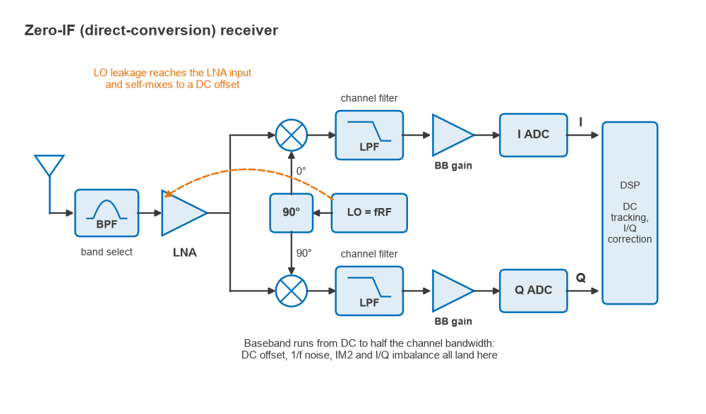
The practical benefits are a lower part count, no off-chip IF filter, a single synthesizer and easy reconfiguration of channel bandwidth simply by changing the baseband filter corners. A multi-band, multi-standard radio becomes far simpler. The costs all arise from the fact that the wanted signal now sits on top of DC and the low-frequency region where many circuit impairments live.
DC Offset and LO Self-Mixing
Any signal at the LO frequency that reaches the RF port of the mixer is mixed with the LO itself and produces a DC term. The LO can leak to the LNA input through substrate coupling, bond wires or the package, reflect off the antenna or filter, and come back in. Equally, a strong blocker that leaks into the LO port mixes with itself. Both paths produce a DC offset that depends on the phase of the leakage, so it changes with frequency, temperature and antenna conditions.
Worked example: how big is the offset?
Assume LO leakage reaches the LNA input at −80 dBm. In a 50 Ω system that is 10−11 W, or an rms voltage of √(10−11 × 50) = 22.4 µV. Suppose the LNA and mixer together provide 30 dB of voltage gain (×31.6) and the baseband chain another 60 dB (×1000). The self-mixing product appears at DC with an amplitude on the order of 22.4 µV × 31.6 × 1000 ≈ 0.71 V, with the exact value set by the leakage phase.
Compare that with a wanted signal at −100 dBm, which is 20 dB smaller than the leakage. The DC term is ten times the signal amplitude, and with a typical ADC full scale of around 1 V peak-to-peak it uses up most of the converter’s range before the signal is even considered. This is why direct-conversion receivers cannot simply apply all their gain and digitize.
The remedies are layered. Careful layout and differential LO routing reduce leakage at the source. AC coupling or a high-pass corner in the baseband removes DC, but it also removes the signal energy near DC, so the corner must be low relative to the channel bandwidth. For a wide OFDM channel with a null subcarrier at DC this is easy. For a narrowband signal such as GFSK, it can eat into the modulation, and some designs use a low-IF variant instead. Most transceivers also run a DC offset calibration, measuring the offset with the LNA off or shorted and injecting a cancelling current via a DAC in the baseband, followed by digital tracking of whatever residue remains.
Flicker Noise
The noise spectral density of MOS transistors rises at low frequency roughly as 1/f. The frequency at which this flicker noise equals the white noise floor is the corner frequency, which can range from tens of kilohertz to over a megahertz in small-geometry CMOS. In a superhet, the IF is far above that corner, so flicker noise is irrelevant. In a zero-IF receiver, the baseband extends from DC up to half the channel bandwidth, and the lower part of it sits in the flicker region.
The impact depends on the ratio of corner frequency to channel bandwidth. A 20 MHz channel with a 200 kHz corner sees only a small fraction of its band affected, and the effective noise figure rises by a few tenths of a dB at most. A 200 kHz channel with the same corner is badly hurt. Designers respond with high gain in the LNA and mixer so that baseband flicker noise is suppressed when referred to the input, passive mixers that carry no DC current, larger devices in the first baseband stage, and bipolar transistors where the process offers them. The noise figure calculation follows the Friis method from Part 4; the only change is that the baseband stage’s noise figure becomes a function of frequency.
Even-Order Distortion and IIP2
Part 3 concentrated on third-order intermodulation, because in a superhet the second-order products of two blockers usually land far from the IF. In a zero-IF receiver, the second-order product of two blockers at f1 and f2 falls at f2 − f1, which is a low frequency and may sit directly in the baseband channel. A single amplitude-modulated blocker does the same thing: squaring its envelope produces a baseband copy of the modulation. Second-order products therefore matter, and the second-order intercept point, IIP2, becomes a headline specification.
With the two-tone definition, the input-referred second-order product for two tones each at Pin dBm is
PIM2 = 2Pin − IIP2
Worked example: required IIP2
Consider a receiver with a 5 MHz channel and a 6 dB noise figure. Its input-referred noise floor is −174 + 10log(5 × 10⁶) + 6 = −174 + 67 + 6 = −101 dBm. Two blockers arrive at −25 dBm each.
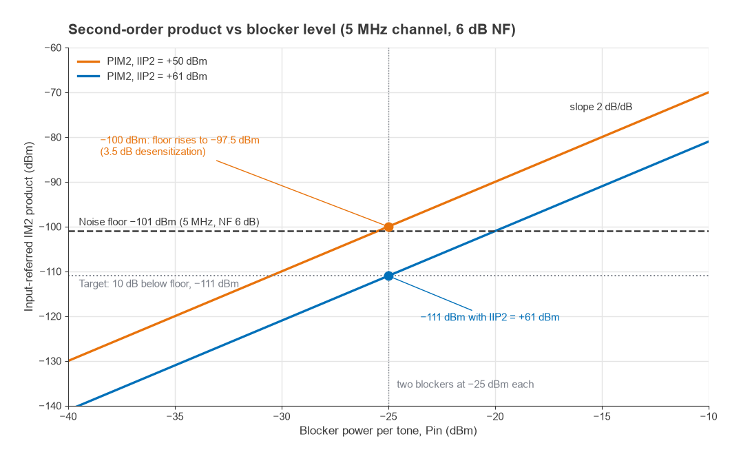
- With IIP2 = +50 dBm, PIM2 = 2(−25) − 50 = −100 dBm, slightly above the noise floor. The receiver is desensitized by about 3.5 dB.
- To push the product 10 dB below the floor, to −111 dBm, the receiver needs IIP2 = 2(−25) − (−111) = +61 dBm.
The desense figure comes from adding −100 dBm to −101 dBm in power: 10log(10−10 + 10−10.1) = −97.5 dBm, which is 3.5 dB above the original floor. Every 1 dB increase in blocker level raises the product by 2 dB, so the required IIP2 climbs quickly with blocker level. In an FDD handset, the receiver’s own transmitter is often the worst offender. Its leakage through the duplexer is a strong modulated signal whose envelope squares down into baseband.
Second-order distortion in a perfectly balanced differential circuit cancels. In practice it is limited by device mismatch and by LO duty-cycle errors in the mixer, so IIP2 varies from part to part. Many transceivers include an IIP2 calibration that trims mixer bias or load balance while a test tone is applied.
I/Q Imbalance and Image Rejection
The I and Q paths should have identical gain and exactly 90° phase difference. When they do not, a signal at a positive baseband frequency +f leaks into its mirror at −f. For a single-carrier signal centred on DC this shows up as a self-image that degrades EVM. For a multicarrier or multichannel signal, a strong carrier at +f can bury a weak one at −f. The ratio of wanted signal to mirror is the image rejection ratio:
IRR = (1 + 2g cosφ + g2) / (1 − 2g cosφ + g2)
where g is the amplitude ratio between the paths and φ is the phase error from quadrature. For small errors this simplifies to IRR ≈ 4 / (ε2 + φ2), with ε = g − 1 and φ in radians.
Worked example: 0.1 dB and 1°
A gain mismatch of 0.1 dB gives g = 100.1/20 = 1.0116, so ε = 0.0116. A phase error of 1° is 0.01745 rad.
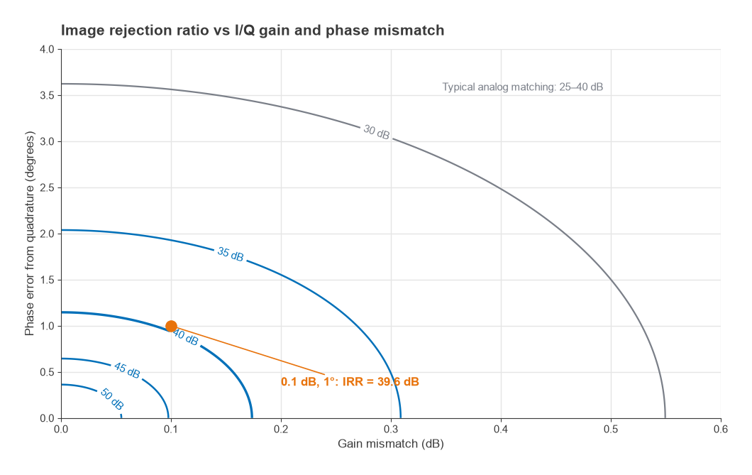
- ε2 = 1.34 × 10⁻⁴, φ2 = 3.05 × 10⁻⁴, sum = 4.39 × 10⁻⁴.
- IRR ≈ 4 / 4.39 × 10−4 = 9120, or 39.6 dB.
The exact formula gives the same 39.6 dB. Note that the 1° phase error contributes more than twice as much as the 0.1 dB gain error. Analog matching on an integrated circuit typically delivers image rejection in the range of 25 to 40 dB. That is adequate for a lot of modulation formats but falls short for dense constellations or for wideband receivers that must handle strong and weak signals side by side. The remainder comes from digital correction: the baseband processor estimates gain and phase mismatch, often from a known test signal or blindly from the statistics of the received data, and applies a 2 × 2 correction matrix. Frequency-dependent imbalance, caused by mismatched baseband filters, needs a short correction filter rather than a single coefficient.
| Impairment | Main cause | Typical mitigation |
|---|---|---|
| DC offset | LO leakage and blocker self-mixing | Layout, AC coupling, offset DAC, digital tracking |
| Flicker noise | 1/f noise in baseband devices | Front-end gain, passive mixers, larger devices |
| Second-order distortion | Mismatch, LO duty-cycle error | Balanced design, IIP2 calibration |
| I/Q imbalance | Gain and phase mismatch between paths | Matching, digital correction |
| LO pulling | PA output coupling into the VCO | Offset VCO frequencies, isolation |
The last row deserves a note. In a transceiver where the transmitter and receiver both use direct conversion, the VCO often runs at twice or some other multiple of the carrier to stop the PA output from pulling it. That multiple is divided down to produce the quadrature LO, which is also a convenient way of generating accurate 90° phases.
Next in the Series
Zero-IF moved the channel filter to baseband. The next step is to remove the mixer altogether and digitize at RF. Part 13, Direct RF Sampling and Software-Defined Radio, covers Nyquist zones, frequency planning for RF ADCs, clock jitter at gigahertz input frequencies and the digital downconversion that turns a wideband converter into a flexible receiver.