

A VCO is designed by pairing a resonant tank with an active circuit whose negative resistance cancels the tank’s losses, then adding a varactor so a control voltage can pull the resonant frequency. VCO design is the branch of oscillator design that sets the topology, tuning gain KVCO and tank Q so the oscillator starts reliably, covers its band and meets its phase noise target.
The voltage-controlled oscillator is the frequency-generating core of almost every PLL frequency synthesizer. The loop corrects slow drift and sets the exact frequency, but outside the loop bandwidth the VCO’s own phase noise reaches the output unchanged, so VCO quality sets much of a synthesizer’s far-out performance. This page explains the negative resistance view of oscillation, the three common topologies, varactor tuning and KVCO, and the trade-offs that link them to phase noise. It sits in the RF oscillators section of the RF design reference.
The negative resistance view
An LC tank on its own rings down, because its series resistance turns stored energy into heat on every cycle. An oscillator adds an active circuit that, looking from the tank, behaves like a negative resistance. If the magnitude of that negative resistance exceeds the tank’s loss resistance, any small disturbance at the resonant frequency grows. The amplitude rises until the active device starts to saturate, its average transconductance falls, and the negative resistance shrinks until it exactly equals the loss. That equilibrium sets the steady-state amplitude.
The condition can be written in series or parallel form:
- Series form: |Rneg| > Rloss, where Rloss is the total series loss of the tank.
- Parallel form: gm,eff × Rp > 1, where Rp is the equivalent parallel tank resistance.
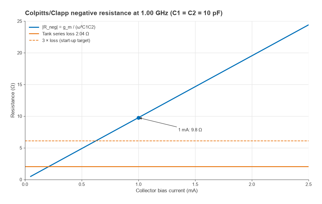
Designers normally provide a start-up margin of about two to three times, so that the oscillator still starts at low temperature, low supply and the worst-case end of the tuning range, where tank Q and device gain are at their lowest. The same impedance view is used for microwave oscillators designed from S-parameters, where the deliberately unstable device is the reverse of the stabilization problem covered in amplifier stability.
Colpitts, Clapp and cross-coupled topologies
Colpitts
The Colpitts oscillator uses a capacitive divider, C1 from base to emitter and C2 from emitter to ground, across a single transistor. Looking into the base, the circuit presents
Zin = −gm / (ω2C1C2) + 1/(jωC1) + 1/(jωC2)
The first term is the negative resistance. An inductor connected across this input resonates with the series combination of C1 and C2. The Colpitts is simple and works well, but its frequency depends partly on the transistor’s internal capacitances, which vary with bias and temperature.
Clapp
The Clapp adds a third capacitor, C3, in series with the inductor. When C3 is much smaller than C1 and C2, it dominates the series combination, so the oscillation frequency is set mainly by L and C3, and the device capacitances, which sit across C1 and C2, have less effect. Placing the varactor in the C3 position makes a tunable Clapp VCO. The frequency is
f0 = 1 / (2π√(L·Ceq)), with 1/Ceq = 1/C1 + 1/C2 + 1/C3
Cross-coupled pair
Integrated VCOs nearly always use a cross-coupled differential pair, in which each transistor’s drain drives the other’s gate. The pair presents a differential resistance of −2/gm across a differential LC tank. Start-up requires 2/gm to be smaller than the differential parallel tank resistance Rp. For example, a 2 nH differential inductor with Q = 15 at 2.4 GHz has Rp = Q·ωL = 15 × 30.2 = 452 Ω, so each device needs gm above 4.4 mS before margin, ignoring varactor loss. The topology is symmetric, gives differential outputs for a mixer or divider, and stacks easily with complementary NMOS and PMOS pairs to reuse current. Its tail current source is a well-known route for low-frequency noise to reach the output, so it is often filtered or replaced by a resistor.
| Topology | Typical use | Strengths | Weaknesses |
|---|---|---|---|
| Colpitts | Discrete VCOs, crystal oscillators | Single device, simple bias | Device capacitance pulls frequency |
| Clapp | Discrete VCOs needing stability | Frequency set mainly by L and C3 | Lower negative resistance, narrower tuning for a given varactor |
| Cross-coupled | RFIC and MMIC VCOs | Differential output, easy start-up, integrable | Tail noise, needs on-chip inductor with modest Q |
Varactor tuning and KVCO
A varactor is a reverse-biased junction whose capacitance falls as the reverse voltage rises:
C(V) = Cj0 / (1 + V/φ)γ
where φ is the built-in potential, about 0.7 V for silicon, and γ is about 0.5 for an abrupt junction. Hyperabrupt varactors use higher values of γ to give a larger capacitance ratio and a more linear frequency-versus-voltage curve. In CMOS processes, accumulation-mode MOS varactors play the same role.
The tuning gain KVCO = df/dV, in MHz/V, is the slope of the tuning curve. It matters in two places. In the PLL, loop bandwidth and stability are proportional to KVCO, so a KVCO that changes by a factor of two across the band changes the loop bandwidth by the same factor, as discussed in PLL loop filter design. In the VCO itself, any noise on the tuning line is multiplied by KVCO and becomes frequency noise.
Worked example: a 1 GHz Clapp VCO
Take L = 10 nH with an inductor Q of 50, C1 = C2 = 10 pF, and an abrupt varactor with Cj0 = 10 pF, φ = 0.7 V and γ = 0.5 in the C3 position.
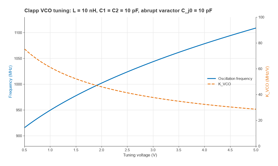
- Centre frequency. At 2 V tuning, C3 = 10/(1 + 2/0.7)0.5 = 5.09 pF. The series combination with C1 and C2 is Ceq = 2.52 pF, so f0 = 1/(2π√(10 nH × 2.52 pF)) = 1002 MHz.
- Tuning range. From 0.5 V to 5 V the varactor moves from 7.64 pF to 3.50 pF and the frequency from 915.6 MHz to 1108.8 MHz, about 19 % of the centre frequency.
- KVCO. The slope is 75 MHz/V at 0.5 V, 46 MHz/V at 2 V and 29 MHz/V at 5 V, a variation of about 2.6 to 1 across the range.
- Tank loss. At 1 GHz the inductor reactance is 63.0 Ω, so its series resistance is 63.0/50 = 1.26 Ω. A varactor Q of 40 adds 1/(ωC3Q) = 0.78 Ω. Total series loss is 2.04 Ω, and the tank Q from these losses is 63.0/2.04 = 30.9.
- Start-up. At 1 mA collector current, gm = IC/VT = 38.7 mS, and Rneg = gm/(ω2C1C2) = 9.76 Ω. That is a margin of 4.8 over the 2.04 Ω loss. A 3 × margin needs only 0.63 mA.
The example ignores transistor capacitances and the loading of the output buffer, both of which lower the frequency and the tank Q in a real circuit. Bias current also sets output amplitude, and with it phase noise, so the final choice is usually above the minimum start-up current. A harmonic-balance simulation, described in harmonic balance simulation, is the normal way to confirm amplitude and frequency before layout. Component self-resonance and parasitics, covered in RF component parasitics, should be checked for every tank part.
Phase noise trade-offs
Leeson’s model gives a useful first estimate of single-sideband phase noise at offset Δf from a carrier f0:
L(Δf) = 10log{ (2FkT/Ps) × [1 + (f0/(2QLΔf))2] × (1 + fc/Δf) }
where F is an effective noise factor of the active device, Ps the signal power in the tank, QL the loaded tank Q and fc the flicker corner. For f0 = 1 GHz, QL = 25, F = 6 dB, Ps = 0 dBm and fc = 50 kHz, the model gives −117.2 dBc/Hz at 100 kHz and −138.7 dBc/Hz at 1 MHz. Halving QL to 12.5 makes both figures 6 dB worse. The model’s parameters are partly empirical, so it predicts trends better than absolute values.
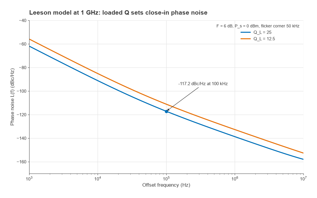
The formula points to the main levers. Phase noise improves as QL2 and in proportion to signal power, so a VCO wants the highest tank Q and the largest swing the devices and supply allow. Wide tuning range works against both: a larger varactor share of the tank capacitance lowers tank Q, since varactors are usually lossier than fixed capacitors, and it raises KVCO.
Tuning-line noise and tuning gain
A noise voltage vn (V/√Hz) on the tuning line frequency-modulates the VCO. For small modulation the resulting phase noise is
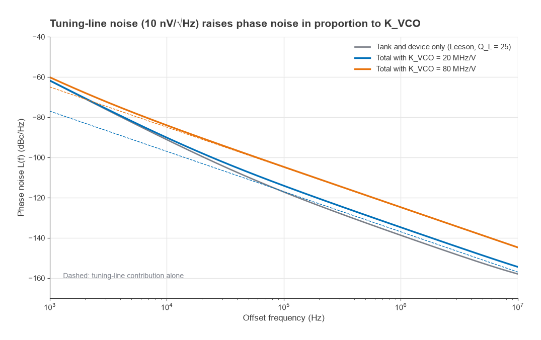
L(Δf) ≈ 20log[KVCO × vn / (√2 × Δf)]
With vn = 10 nV/√Hz, typical of a resistor of a few kilohms in a loop filter, and KVCO = 20 MHz/V, this contributes −117.0 dBc/Hz at 100 kHz, about equal to the tank noise of the example above, and the total is −114.1 dBc/Hz. At KVCO = 80 MHz/V the tuning-line term is −104.9 dBc/Hz and dominates, giving a total of −104.7 dBc/Hz. This is why wideband VCOs split their range into switched capacitor bands, each with a small KVCO, rather than relying on one large varactor.
VCO design steps
- Set frequency range, phase noise at key offsets, output power, supply and current budget.
- Choose the topology: Clapp or Colpitts for discrete designs, cross-coupled for integrated ones.
- Choose the inductor for the highest practical Q, then size fixed and variable capacitance for the range plus margin for process and temperature.
- Calculate KVCO across the range; if it is too high or varies too much, add switched capacitor bands.
- Calculate tank loss and set bias for a start-up margin of two to three at the worst corner.
- Estimate phase noise with Leeson’s model and the tuning-line term, then simulate and measure.
- Add a buffer to isolate the tank from load changes, which otherwise pull the frequency.
Measurement methods for the finished oscillator are covered in phase noise measurement.
Frequently asked questions
How do you design a VCO?
Choose a topology and an LC tank that resonates at the centre frequency, add a varactor sized for the tuning range, and bias the active device so its negative resistance exceeds the tank loss by two to three times. Then check KVCO and phase noise against the requirements and iterate on tank Q, swing and tuning range.
What is KVCO?
KVCO is the VCO’s tuning sensitivity, the change in output frequency per volt of tuning voltage, usually in MHz/V. It sets the gain of the PLL loop and determines how much tuning-line noise is converted into phase noise.
Why does a wider tuning range worsen phase noise?
A wider range needs a larger varactor share of the tank, which usually lowers tank Q, and a higher KVCO, which amplifies noise on the tuning line. Both degrade phase noise. Band switching recovers much of the loss by keeping KVCO small within each band.
What is the difference between a Colpitts and a Clapp oscillator?
A Clapp is a Colpitts with an extra small capacitor in series with the inductor. That capacitor dominates the tank capacitance, so transistor capacitances have less effect on frequency and stability improves, at the cost of less negative resistance and a narrower tuning range for a given varactor.
Related topics
The reference oscillators that discipline a VCO inside a PLL are compared in TCXO vs OCXO, and an alternative digital approach to frequency generation is described in direct digital synthesis. Tank Q is explained in Q factor in RF circuits, and short definitions are in the wireless terms glossary.