

Part 9 covered the filters that keep unwanted signals out of the transmit and receive paths. One signal cannot be filtered away, because the radio generates it deliberately and feeds it straight into the mixers: the local oscillator. Any noise or spurious content on the LO is transferred onto every signal the mixer handles. In a receiver it lets strong neighboring signals spill into the wanted channel; in a transmitter it adds directly to EVM and to the noise emitted in adjacent channels.
Part 2 introduced LOs and mixers as functional blocks. This part looks at how LOs are actually generated, using phase-locked loop (PLL) synthesizers, and at the quantity that dominates their quality: phase noise.
The Integer-N PLL
A PLL synthesizer locks a voltage-controlled oscillator (VCO) to a stable crystal reference. The VCO output is divided by N and compared with the reference (itself possibly divided by R) in a phase-frequency detector (PFD). The PFD drives a charge pump, whose output current pulses are integrated and smoothed by the loop filter to produce the VCO tuning voltage. In lock, the divided VCO matches the reference in frequency and phase, so
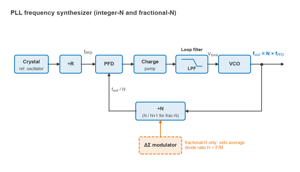
fout = N × fPFD, where fPFD = fref / R
In an integer-N synthesizer, N is a whole number, so the output can only step in increments of fPFD. The channel spacing therefore sets the comparison frequency. A 200 kHz channel raster at 900 MHz requires fPFD = 200 kHz and N = 4500.
That large N is the core problem with integer-N designs. Inside the loop bandwidth, the PLL forces the VCO phase to follow the reference and PFD, so their noise appears at the output multiplied by N. Since phase noise is a power ratio of phase fluctuations, the multiplication adds 20 log10 N dB. A low comparison frequency also forces a narrow loop bandwidth, typically no more than about a tenth of fPFD to keep the loop stable and suppress reference spurs, which slows settling.
Fractional-N Synthesis
A fractional-N synthesizer lets the divide ratio take non-integer average values. The divider switches between N and N + 1 (or across a wider range of integers) in a pattern whose average is N + F/M. The output can then step in increments far finer than fPFD, so the comparison frequency can be made much higher.
Switching the divider periodically would create large spurious tones at multiples of the fractional offset. Modern designs drive the divider with a delta-sigma modulator, which randomizes the switching sequence and pushes its quantization noise to high offset frequencies, where the loop filter attenuates it. Two residual problems remain. The shaped quantization noise rises with offset, so it must be filtered by the loop, which limits how wide the loop can be. And nonlinearity in the charge pump and PFD folds some of that high-frequency noise back down, producing fractional spurs, which are worst when the output lies close to an integer multiple of fPFD (integer-boundary spurs).
Worked Example: In-Band Noise, Integer-N Versus Fractional-N
The in-band phase noise floor of a PLL can be estimated from a normalized figure of merit, the phase noise the PFD and charge pump would produce at 1 Hz comparison frequency with N = 1:
Lin-band = Lnorm + 10 log10(fPFD) + 20 log10(N)
Assume Lnorm = −220 dBc/Hz and an output at 900 MHz.
- Integer-N, fPFD = 200 kHz, N = 4500: −220 + 53.0 + 73.1 = −93.9 dBc/Hz.
- Fractional-N, fPFD = 50 MHz, N = 18: −220 + 77.0 + 25.1 = −117.9 dBc/Hz.
The fractional-N loop is 24 dB quieter in band. The 10 log term increases with comparison frequency while the 20 log term falls faster, so raising fPFD by a factor k improves in-band noise by 10 log10 k. Here k = 250, giving 24.0 dB. The higher fPFD also allows a wider loop bandwidth, which speeds settling and suppresses more of the VCO’s own noise.
The reference oscillator is multiplied the same way. A 10 MHz crystal oscillator with −150 dBc/Hz at 10 kHz offset, multiplied to 2.4 GHz (a factor of 240), contributes −150 + 20 log10(240) = −150 + 47.6 = −102.4 dBc/Hz at that offset, if 10 kHz lies inside the loop bandwidth. A synthesizer can never be quieter in band than its reference multiplied up to the output.
Phase Noise and the VCO
Phase noise is specified as L(Δf), the single-sideband noise power in a 1 Hz bandwidth at an offset Δf from the carrier, relative to the carrier power, in dBc/Hz. Outside the loop bandwidth the VCO is effectively free-running, so its own noise dominates.
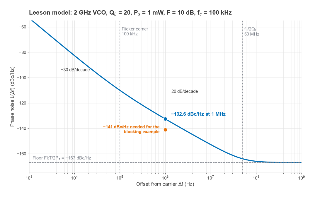
Leeson’s model describes the VCO’s phase noise in terms of the resonator’s loaded Q (QL), the signal power in the resonator Ps, the active device’s effective noise factor F, and its flicker noise corner fc:
L(Δf) = 10 log10 { (F k T / 2Ps) [ 1 + (f0 / (2 QL Δf))2 ] (1 + fc/Δf) }
The squared term gives the familiar 20 dB per decade slope inside the resonator’s half-bandwidth, f0/(2QL). Below the flicker corner the slope steepens to 30 dB per decade. Far from the carrier the curve flattens to a floor set by F k T / 2Ps.
As an example, take f0 = 2 GHz, QL = 20 (representative of an integrated LC tank), Ps = 1 mW, F = 10 dB and fc = 100 kHz. At Δf = 1 MHz, f0/(2QLΔf) = 2×10⁹ / (40 × 106) = 50, so the bracket is 1 + 2500 = 2501, or 34.0 dB. The flicker term is 1.1, or 0.4 dB. F k T / Ps is −174 dBm/Hz + 10 dB − 0 dBm = −164 dB in a 1 Hz bandwidth, and the factor of one half takes off 3.0 dB. The total is
L(1 MHz) = −164 − 3.0 + 34.0 + 0.4 ≈ −132.6 dBc/Hz
Doubling QL improves this by close to 6 dB, and doubling the signal power by 3 dB. These are the levers a VCO designer has, and both are limited: Q by the inductor and varactor technology, power by supply voltage and device breakdown.
Choosing the Loop Bandwidth
Inside the loop bandwidth the loop suppresses VCO noise and passes the multiplied reference and PFD noise. Outside, it does the opposite. To minimize total integrated noise, the loop bandwidth is placed near the offset where the in-band floor and the free-running VCO curve cross. A loop that is too narrow leaves the VCO’s close-in noise uncorrected; one that is too wide passes more delta-sigma quantization noise and reference spurs. Settling time, which falls roughly in inverse proportion to loop bandwidth, often pushes the choice wider than the noise optimum.
From Phase Noise to Jitter and EVM
A single phase noise number at one offset says little about how a modulated signal will suffer. What matters is the total phase error integrated over the offsets that affect the demodulator, roughly from the carrier tracking bandwidth out to the edge of the channel. The RMS phase error in radians is
φrms = √( 2 ∫ 10L(f)/10 df )
The factor of 2 accounts for both sidebands. RMS jitter at carrier frequency f0 is tj = φrms / (2π f0), and for small errors the EVM contribution is approximately φrms expressed as a percentage.
Worked Example
Take a 2.4 GHz synthesizer whose phase noise is approximately flat at −100 dBc/Hz from 1 kHz to 1 MHz, and negligible elsewhere. The integration bandwidth is close to 1 MHz, so the integrated single-sideband noise is −100 + 10 log10(106) = −40 dBc, or 10−4. Then
- φrms = √(2 × 10⁻⁴) = 0.0141 rad = 0.81°
- tj = 0.0141 / (2π × 2.4 × 109) ≈ 0.94 ps RMS
- EVM contribution ≈ 1.41%
This is the figure used in the transmitter EVM budget of Part 6. For 256-QAM or 1024-QAM, where total EVM targets are a few percent or less, a phase noise contribution of 1.4% is already a large share of the budget. Higher-order modulation and higher carrier frequencies both raise the bar on synthesizer design, since multiplying an LO up to millimeter-wave frequencies adds 20 log10 of the multiplication factor to its phase noise.
Reciprocal Mixing and Spurs
In a receiver, LO phase noise does more than degrade the wanted signal. A strong signal in a nearby channel mixes with the LO’s noise skirt and lands in the IF passband on top of the wanted signal. This is reciprocal mixing, and it often limits blocking performance more than the mixer’s linearity does. The noise added is
PRM = Pblocker + L(Δf) + 10 log10(B) dBm
where Δf is the blocker’s offset and B the channel noise bandwidth.
Worked Example: Phase Noise Required for Blocking
A receiver with a 200 kHz channel and a 7 dB noise figure has a noise floor of −174 + 53.0 + 7 = −114 dBm, using the kTB approach of Part 4. It must tolerate a −26 dBm blocker at 1 MHz offset. If reciprocal mixing is allowed to add noise equal to the thermal floor (a 3 dB sensitivity loss), then
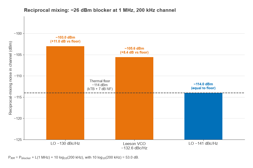
−26 + L(1 MHz) + 53.0 ≤ −114, so L(1 MHz) ≤ −141 dBc/Hz
An LO with −130 dBc/Hz at 1 MHz would produce −26 − 130 + 53 = −103 dBm of reciprocal mixing noise, 11 dB above the thermal floor, and the receiver would fail the blocking test by a wide margin. The VCO from the Leeson example, at −132.6 dBc/Hz, would also fall short. Meeting −141 dBc/Hz needs a higher-Q resonator, more signal swing, or a VCO running at a multiple of the LO frequency and divided down, since division by M improves phase noise by 20 log10 M.
Discrete spurs behave the same way. A reference spur at −70 dBc, offset by fPFD, will translate any blocker at that offset into the channel 70 dB down. Spurs are therefore specified against the blocking profile of the standard, not just as an absolute level.
| Noise or spur source | Region where it dominates | Main remedy |
|---|---|---|
| Reference oscillator | Close in, inside loop bandwidth | Cleaner reference, lower multiplication |
| PFD and charge pump | Inside loop bandwidth | Higher fPFD, better figure of merit |
| Delta-sigma quantization | Near and beyond loop bandwidth | Higher-order loop filter, narrower loop |
| VCO | Outside loop bandwidth | Higher Q, more swing, divide-down |
| Reference and fractional spurs | At fPFD multiples and near integer boundaries | Loop filtering, frequency planning, dithering |
Next in the Series
The synthesizer clocks the mixers, and an equally clean clock is needed by the data converters. Part 11, DACs and the Transmit Signal Chain, returns to the transmitter’s digital edge: DAC resolution and SFDR, sinc roll-off and images, interpolation, and how clock jitter limits the signal-to-noise ratio of a high-speed DAC.