

A capacitor acts like an inductor at high frequency because its leads, terminations, internal electrodes and mounting pads carry current through a physical loop, and that loop has inductance, the equivalent series inductance (ESL). Above the self-resonant frequency (SRF), where the reactance of the ESL cancels the reactance of the capacitance, the part’s impedance rises with frequency like an inductor.
Every passive component has parasitics of this kind. Capacitors have series inductance and resistance, inductors have capacitance between their turns, and resistors have both. At audio frequencies these are negligible. In the hundreds of megahertz and above they decide whether a decoupling capacitor decouples, whether a bias choke chokes, and whether a matching network lands where the simulation says it should. This page covers the equivalent circuits, self-resonance, package size and the choice between inductor technologies, as part of the RF fundamentals section of the RF design reference.
Equivalent circuits of real components
A simple equivalent circuit captures most of the behaviour of a surface-mount part up to and a little beyond its first resonance. Manufacturers’ detailed models or measured S-parameters should be used for final design, but the simple forms explain what happens.
| Component | Simple equivalent circuit | Dominant parasitic | First resonance |
|---|---|---|---|
| Capacitor | C in series with ESL and ESR | ESL | Series resonance, minimum |Z| = ESR |
| Inductor | L in series with Rs, all shunted by Cp | Inter-winding capacitance Cp | Parallel resonance, maximum |Z| |
| Resistor | R in series with Ls, shunted by Cp | Ls for low R, Cp for high R | Usually above the useful range for small chips |
The equivalent series resistance (ESR) of a capacitor comes from electrode and termination metal and from dielectric loss. It rises with frequency as skin effect confines current to the surface of the conductors. Inductor series resistance Rs behaves the same way. These resistances set the component Q factor, which in turn sets the loss of any filter or matching network built from the parts.
Capacitor self-resonant frequency
For the series model the impedance is Z = ESR + jωESL + 1/(jωC). The reactive terms cancel at
fSRF = 1 / (2π √(ESL × C))
Below the SRF the part is capacitive, though its effective capacitance is larger than nominal: Ceff = C / (1 − (f/fSRF)2). At the SRF its impedance falls to ESR. Above it the part is inductive, and its impedance approaches ωESL regardless of the capacitance value.
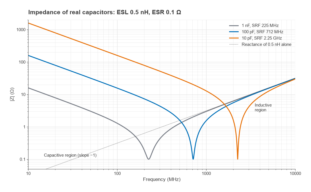
With an ESL of 0.5 nH, a value in the range often quoted for small chip capacitors once pads are included, the SRF is 225 MHz for 1 nF, 712 MHz for 100 pF and 2.25 GHz for 10 pF. At 1 GHz the 10 pF part already behaves like 12.5 pF. These values assume a constant ESL, which is a reasonable approximation because ESL depends mainly on the package and mounting rather than the capacitance.
Worked example: a DC block at 2.4 GHz
A designer needs a series DC-blocking capacitor in a 50 Ω line at 2.4 GHz and reaches for 100 pF on the basis that “bigger is better”. With ESL = 0.5 nH:
- Inductive reactance: XL = 2π × 2.4 × 109 × 0.5 × 10−9 = 7.54 Ω.
- Capacitive reactance: XC = 1 / (2π × 2.4 × 109 × 100 × 10−12) = 0.66 Ω.
- Net reactance: +6.88 Ω. The 100 pF capacitor is a 0.46 nH inductor at this frequency.
Choosing C so that the SRF falls on the operating frequency gives C = 1 / ((2πf)2 × ESL) = 8.8 pF. A standard 10 pF part leaves a net reactance of only +0.91 Ω, a much smaller disturbance to the line. The same reasoning applies to RF bypass capacitors on bias lines, which work best when their series resonance is near the frequency they must short to ground.
Decoupling across a wide band
A single capacitor gives low impedance only near its SRF. Power supply decoupling for RF circuits therefore combines several values, for example a small capacitor close to the device pin for the RF band and larger values further out for lower frequencies. Paralleled capacitors create an anti-resonance between them, where the inductance of the larger part resonates with the capacitance of the smaller one and the combined impedance peaks. Keeping ESL low, using several vias to ground, and checking the combined impedance curve are the usual remedies. The RF power supply decoupling page covers layout in detail.
Package size: 0201, 0402 and 0603
ESL scales with the current loop, so smaller packages have lower inductance. As an approximate guide, mounted chip capacitors fall somewhere around 0.3 nH for 0201, 0.4 to 0.5 nH for 0402 and 0.6 to 0.9 nH for 0603, with the pad and via geometry adding a significant share. The effect on SRF follows the square root: for a 10 pF capacitor, an ESL of 0.30 nH gives an SRF of 2.91 GHz, 0.45 nH gives 2.37 GHz and 0.70 nH gives 1.90 GHz.
Smaller is not always better. Smaller parts have lower parasitic capacitance to ground and lower ESL, and they fit the narrow traces of high-frequency RF PCB layout. They also have lower power and voltage ratings, are harder to rework, and come in a narrower range of values. Pad geometry matters as much as the part: a 0402 capacitor on oversized pads can show more parasitic capacitance than the trace it sits on.
Dielectric type matters too. Class 1 ceramics such as C0G (NP0) have low loss and almost no change in capacitance with voltage or temperature, which makes them the normal choice in matching networks and filters. Class 2 ceramics such as X7R pack more capacitance into the same size but lose capacitance under DC bias and have higher loss, so they belong in decoupling and bulk bypass roles.
Inductor parasitics and self-resonance
An inductor’s turns sit next to each other and next to the ground plane, and the capacitance between them appears in parallel with the winding. The inductor resonates when that capacitance Cp cancels the inductance, fSRF = 1/(2π√(L Cp)). Below the SRF the effective inductance rises as Leff ≈ L / (1 − (f/fSRF)2). At the SRF the impedance peaks and is purely resistive. Above it the part behaves as a capacitor.
A 10 nH inductor with 0.1 pF of parallel capacitance has an SRF of 5.03 GHz. At 2.4 GHz its effective inductance is already 10 / (1 − (2.4/5.03)2) = 12.9 nH, nearly 30% above nominal. A matching network designed with the nominal value would be noticeably off. The practical rule is to use inductors well below their SRF in matching and filter circuits, and to make sure the datasheet value is quoted at a frequency close to the one in use.
The opposite choice applies to RF chokes. A bias feed inductor should present a high impedance at the operating frequency, and the highest impedance it ever reaches is at its parallel resonance. Choosing an inductor whose SRF sits near the operating frequency makes the choke more effective, as discussed in RF amplifier biasing.
Wire-wound versus multilayer inductor Q
Inductor Q, ωL/Rs at low frequency, depends on the conductor. Wire-wound chip inductors use a solid copper wire on a ceramic or air core. Multilayer inductors print thin metal traces between ceramic layers. Thin film inductors use photolithographic traces with very tight tolerance. The wire carries current through a larger cross-section, so wire-wound parts typically reach higher Q, often several times that of a multilayer part of the same value and size, at the cost of higher price and a slightly larger footprint.
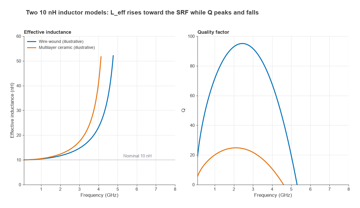
The two illustrative models in Figure 2 show the effect. Both are 10 nH. The wire-wound model has Rs = 0.85 Ω at 1 GHz, giving Q = 71, and reaches a peak Q of 95 near 2.4 GHz. The multilayer model has Rs = 3.0 Ω at 1 GHz, giving Q = 20, with a peak of 25 near 2.1 GHz. In both, Q rises at first because reactance grows faster than skin-effect resistance, then falls to zero at the SRF as the parallel capacitance takes over. In a filter, that difference in Q can be the difference between 1 dB and 3 dB of loss, as the filter specifications page shows.
Resistor parasitics
A chip resistor has a small series inductance from its length and terminations, and a small parallel capacitance across its body and pads. The ratio √(Ls/Cp) marks the resistance that stays flattest with frequency. With Ls = 0.4 nH and Cp = 0.05 pF it is 89 Ω, which is why resistors in the tens of ohms behave well at RF.
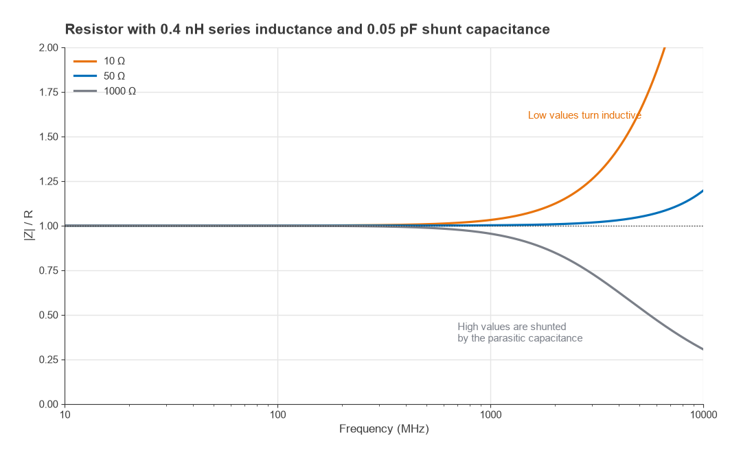
Away from that value the parasitics show up. In the model, a 50 Ω resistor has |Z| = 50.1 Ω at 1 GHz and 52.4 Ω at 5 GHz, with a phase of 9.5°. A 10 Ω resistor reaches 16.4 Ω at 5 GHz with a 51° phase angle, because its series inductance dominates. A 1 kΩ resistor drops to 540 Ω at 5 GHz, shunted by its own capacitance. Thin film resistors on suitable substrates, and specialised terminations with controlled geometry, are used where a resistor must stay resistive into the microwave range, such as attenuators and loads.
Choosing RF capacitors and inductors
- Check the SRF against the operating frequency for every part. For DC blocks and bypass capacitors, aim for the series resonance near the operating band. For matching and filter elements, stay well below the SRF.
- Use the manufacturer’s S-parameter or model data in simulation, measured on a known pad layout, rather than nominal values.
- Prefer C0G/NP0 capacitors in signal paths and high-Q wire-wound or thin film inductors where loss matters.
- Keep pads small and vias short, because they add to the part’s parasitics.
- Remember tolerance. A ±0.1 pF tolerance on a 1 pF capacitor is 10%, and that can move a resonance more than the parasitics do.
These considerations shape every lumped L-network and LC filter. Above a few gigahertz the parasitics become comparable with the intended values, and designers move to distributed elements built from transmission lines.
Frequently asked questions
Why does a capacitor act like an inductor at high frequency?
Current through any real capacitor flows around a physical loop formed by its electrodes, terminations and pads, and that loop has inductance. Above the self-resonant frequency the inductive reactance exceeds the capacitive reactance, so the part’s impedance rises with frequency, just as an inductor’s does.
What is self-resonant frequency?
It is the frequency at which a component’s intended reactance and its parasitic reactance cancel. For a capacitor it is the series resonance of C and ESL, where impedance falls to the ESR. For an inductor it is the parallel resonance of L and inter-winding capacitance, where impedance peaks.
How do I choose RF capacitors and inductors?
Start from the role. Blocking and bypass capacitors should resonate near the operating frequency. Tuning and matching parts should operate well below their SRF, with high Q and tight tolerance. Then confirm the choice with the manufacturer’s measured data on the actual pad layout.
Does a smaller package always give better RF performance?
Smaller packages have lower ESL and parasitic capacitance, so their resonances are higher. They also handle less power and voltage and have a smaller range of values, so the best package is the smallest one that meets the electrical and mechanical requirements.
Related topics
Component loss is quantified on the Q factor page and its physical cause on the skin effect page. Impedances that move with frequency are easiest to follow on a Smith chart. Short definitions of ESR, ESL and SRF are in the wireless terms glossary.