

RF supply decoupling is the set of capacitors, ferrite beads, regulators and layout choices that keep supply noise out of sensitive RF circuits and keep RF currents off the supply rails. To decouple an RF IC, place a small capacitor whose self-resonant frequency is near the operating frequency right at each supply pin, back it with larger capacitors for lower frequencies, and feed the rail through an LDO or a damped ferrite-bead filter. Every capacitor needs a short, low-inductance path to ground.
This page belongs to the RF PCB layout section of the RF design guide. It covers capacitor self-resonance, why parallel capacitors can make things worse, how ferrite beads and LDOs fit in, and how switching-regulator ripple turns into spurs on an oscillator or power amplifier output.
What decoupling has to do at RF
A supply decoupling network has three jobs. It must provide a low impedance at the RF frequency so that RF current drawn by the device circulates locally instead of travelling along the supply trace. It must block noise and ripple coming from the regulator and other circuits, from audio frequencies to the switching frequency of a DC-DC converter and its harmonics. And it must prevent coupling between stages that share a rail, which can otherwise create feedback paths and oscillation in a multi-stage amplifier.
No single component covers all of that. Capacitors work over a band set by their self-resonance, beads and inductors add series impedance over another band, and linear regulators reject noise mainly at low frequencies. A good design layers them so the bands overlap.
Capacitor self-resonant frequency selection
A real capacitor is a series RLC: the capacitance C, an equivalent series resistance (ESR) and an equivalent series inductance (ESL) that includes the package, the pads and the via to ground. Its impedance is:
Z = ESR + j(ωLESL − 1/(ωC))
Below the self-resonant frequency it behaves as a capacitor. Above it, it behaves as an inductor. At resonance the reactances cancel and the impedance falls to the ESR:
fSRF = 1 / (2π √(LESL C))
The mounted inductance matters as much as the capacitor itself. A small case size, wide short pads and a via placed inside or right next to the pad all help. The via contribution can be estimated as shown in grounding and via stitching, and component parasitics in general are covered in RF component parasitics.
Worked example: choosing the RF bypass capacitor for 2.4 GHz
Assume a total mounted inductance of 0.6 nH for a small ceramic capacitor and its ground via. This is an illustrative value; datasheet models and EM simulation give the real figure for a given part and layout.
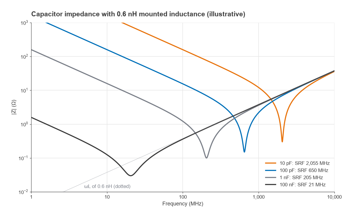
- The capacitance that resonates at 2.4 GHz is C = 1 / ((2πf)2 L) = 1 / ((2π × 2.4 × 109)2 × 0.6 × 10−9) = 7.3 pF.
- The nearest common value, 6.8 pF or 8.2 pF, gives a low impedance across the 2.4 GHz band.
- A 100 pF capacitor with the same 0.6 nH resonates at 650 MHz. At 2.4 GHz its reactance is 9.05 − 0.66 = 8.4 Ω inductive, so it is a poor RF bypass at that frequency.
- Larger values move the SRF down: 1 nF at 205 MHz and 100 nF at 21 MHz with the same mounting.
Above its SRF every capacitor in this example follows the same ωL line. Once the value is large enough to resonate below the frequency of interest, a bigger capacitor gives no further help there. Only lower inductance does.
Parallel capacitors and antiresonance
Designers often parallel a large and a small capacitor to cover a wide band. Between the two SRFs, though, the large capacitor is already inductive while the small one is still capacitive, and together they form a parallel resonant tank. With 100 nF and 100 pF, each with 0.6 nH, the combined impedance peaks at about 459 MHz and 16.7 Ω, much higher than either part alone at that frequency. If a circuit on the board operates or radiates near 459 MHz, the “better” decoupling is worse there.
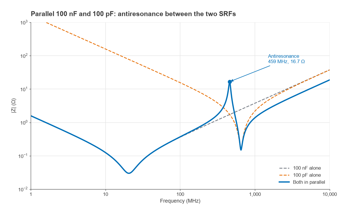
Antiresonance can be managed by spacing capacitor values closely (for example by factors of three to ten rather than a thousand), by using parts with some ESR to damp the peak, or by choosing values so the peak falls where nothing sensitive operates. Simulating the network with real capacitor models is the reliable check.
Ferrite beads and LC supply filters
A ferrite bead behaves as a small inductor at low frequency and as a resistor over its rated band, typically tens to hundreds of megahertz. The resistive region is useful: it absorbs RF energy instead of reflecting it. A bead in series with the supply and a capacitor to ground at the IC side form a low-pass filter.
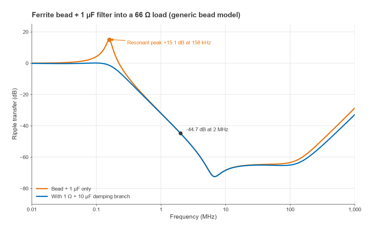
The hazard is the low-frequency inductance. A bead with roughly 1 µH of low-frequency inductance and a 1 µF capacitor resonate at 1 / (2π√(1 µH × 1 µF)) = 159 kHz. With a lightly loaded rail, the filter has gain at that frequency. In the generic model behind Figure 3, feeding a 66 Ω load (about 50 mA at 3.3 V), the peak is +15.1 dB at 158 kHz. Any supply noise near that frequency is amplified, not filtered.
Adding a damping branch, here 1 Ω in series with 10 µF across the filter capacitor, reduces the peak to about 0.1 dB while leaving the high-frequency attenuation almost unchanged. At 2 MHz, a common DC-DC switching frequency, this filter attenuates by 44.7 dB. Two further cautions apply. Bead impedance drops with DC current as the ferrite saturates, so a bead that looks good unbiased may do little on a PA rail carrying hundreds of milliamps. And a bead with a capacitor only on one side relies on the source and load impedances that surround it, which vary with operating mode.
LDO PSRR
A low-dropout regulator’s power supply rejection ratio (PSRR) is the ratio of input ripple to output ripple, in dB. It is high at low frequency, often 60 dB or more, because the regulator’s feedback loop has plenty of gain there. As frequency rises the loop gain falls and PSRR drops, commonly to somewhere in the 20 to 40 dB range around 1 MHz for general-purpose parts, with the output capacitor and layout taking over above that. Parts designed for RF and clock supplies hold their PSRR to higher frequencies, but the datasheet curve at the actual ripple frequency, load current and dropout voltage is the number to use.
LDO output noise also matters, separately from PSRR. A VCO, a PLL charge pump or a low-noise amplifier bias network converts supply noise directly into phase noise or gain modulation, so these rails often get the lowest-noise regulator on the board.
Switching-spur coupling into the LO and PA
Switching regulators are efficient but leave ripple at the switching frequency fsw and its harmonics, plus fast edge noise. Supply ripple reaches the RF output through two main mechanisms.
- Oscillator pushing. A VCO’s frequency shifts with supply voltage by its pushing figure Kpush in Hz/V. Ripple of peak amplitude Vr at fsw frequency-modulates the carrier with index β = KpushVr / fsw. For small β the sidebands at ±fsw sit at 20log(β/2) dBc. A PLL suppresses pushing inside its loop bandwidth, but ripple above the loop bandwidth passes through. The effect on the spectrum is the same as discrete phase noise spurs.
- PA supply modulation. In a saturated power amplifier the output amplitude roughly follows the supply voltage. Ripple with modulation index m = Vr/VDD produces AM sidebands at 20log(m/2) dBc. Linear PAs are less sensitive, but AM-to-PM conversion adds phase sidebands too.
Worked example: a 2 MHz buck feeding a VCO and a PA
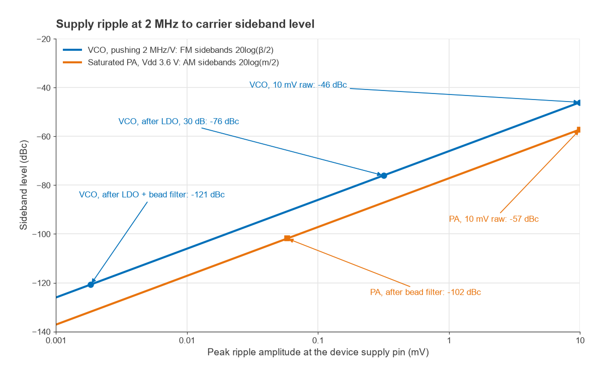
Assume a buck converter at fsw = 2 MHz with 10 mV peak ripple, a VCO with an assumed pushing of 2 MHz/V outside the PLL bandwidth, and a saturated PA running from 3.6 V. The LDO is assumed to give 30 dB PSRR at 2 MHz, and the bead filter above gives 44.7 dB.
| Path | Ripple at pin (peak) | Modulation | Sideband at ±2 MHz |
|---|---|---|---|
| VCO, raw buck output | 10 mV | Δf = 20 kHz, β = 0.01 | −46 dBc |
| VCO, after LDO | 0.316 mV | Δf = 632 Hz, β = 3.16 × 10⁻⁴ | −76 dBc |
| VCO, after LDO and bead filter | 1.84 µV | Δf = 3.7 Hz, β = 1.84 × 10⁻⁶ | −121 dBc |
| PA, raw buck output | 10 mV | m = 2.78 × 10⁻³ | −57 dBc |
| PA, after bead filter | 58 µV | m = 1.62 × 10⁻⁵ | −102 dBc |
For the first row, Δf = 2 × 10⁶ Hz/V × 0.01 V = 20 kHz and β = 20 × 103 / 2 × 106 = 0.01, so the sideband is 20log(0.005) = −46.0 dBc. Each stage of filtering lowers the spur dB for dB. Whether −76 dBc is enough depends on the system: a spur at ±2 MHz falls in or near adjacent channels for many standards, and it also mixes with strong blockers in a receiver LO. The spurs also appear at harmonics of fsw, where the filter usually helps more.
Layout matters as much as filtering. The buck’s switch node and input capacitor loop should be compact and far from the LO, the PA output and the antenna. A fast switch edge couples through stray capacitance and through the ground plane even when the rail itself is clean, which is why switching converters are often placed under a shield or on the opposite side of the board.
Step-by-step decoupling of an RF IC
- List each supply pin, its function (LO, PA, LNA, digital) and its sensitivity.
- Place an RF bypass capacitor with SRF near the operating frequency at each pin, with its ground via inside or next to the pad.
- Add a mid-value capacitor (roughly 1 to 100 nF) per rail for lower frequencies, checking the antiresonance with the RF capacitor.
- Feed sensitive rails (VCO, PLL, LNA) from a low-noise LDO with adequate PSRR at the switching frequency.
- Add a bead or inductor filter where needed, with a damping branch, and check bead impedance at the real DC current.
- Calculate the expected spur levels from ripple, pushing and PA sensitivity, and compare them with the spectral mask.
- Verify on hardware with a spectrum analyzer, looking for sidebands at ±fsw and its harmonics.
Frequently asked questions
How do you decouple an RF IC?
Put a small capacitor with a self-resonant frequency near the operating frequency directly at each supply pin, with a short via to a solid ground plane. Back it with larger capacitors for lower frequencies and feed the rail through an LDO or a damped bead filter. Then check the network for antiresonance peaks.
Do switching regulators hurt RF performance?
They can. Ripple at the switching frequency modulates oscillators and power amplifiers and appears as spurs at ±fsw around the carrier, and fast switching edges radiate. With adequate filtering, an LDO for sensitive rails and careful placement, switching regulators are widely used in RF products.
Why use a small capacitor for RF bypassing instead of a large one?
Above its self-resonant frequency a capacitor is inductive, and its impedance depends on mounted inductance rather than capacitance. A small value resonates near the RF frequency and gives the lowest impedance there. A large value resonates far below and is just an inductor at RF.
Related topics
Stack-up choices that set plane spacing are compared in FR-4 vs Rogers, and board-level emission control is covered in RF EMC and EMI. How oscillator spurs and noise degrade a radio is explained in PLL frequency synthesis, and the terms used here are defined in the wireless terms glossary.