

A microstrip line is a planar transmission line formed by a conducting strip on one side of a dielectric substrate with a ground plane on the other, and its characteristic impedance depends on the strip width W, the substrate height h and the relative permittivity εr. To calculate it, find the effective permittivity εeff from W/h and εr, then apply the Hammerstad closed-form equations for Z0. The calculator on this page does both directions: impedance from width, and width from a target impedance.
Microstrip is the default interconnect on RF printed circuit boards because it is easy to fabricate, easy to probe and easy to attach components to. It belongs to the transmission line theory section of the RF design map, alongside the general types of transmission lines and the line parameters that the formulas below summarize.
Microstrip Geometry and the Quasi-TEM Mode
In a coaxial cable or a stripline, the field lives entirely in one dielectric and the wave is pure TEM. Microstrip is different. Most of the electric field runs straight down through the substrate, but part of it fringes through the air above the strip. Because the wave travels partly in air and partly in dielectric, it cannot be pure TEM. At the frequencies where microstrip is normally used, the longitudinal field components are small, and the line behaves as if it were a TEM line filled with a single uniform material of permittivity εeff, where 1 < εeff < εr. This is the quasi-TEM approximation, and every closed-form microstrip formula relies on it.
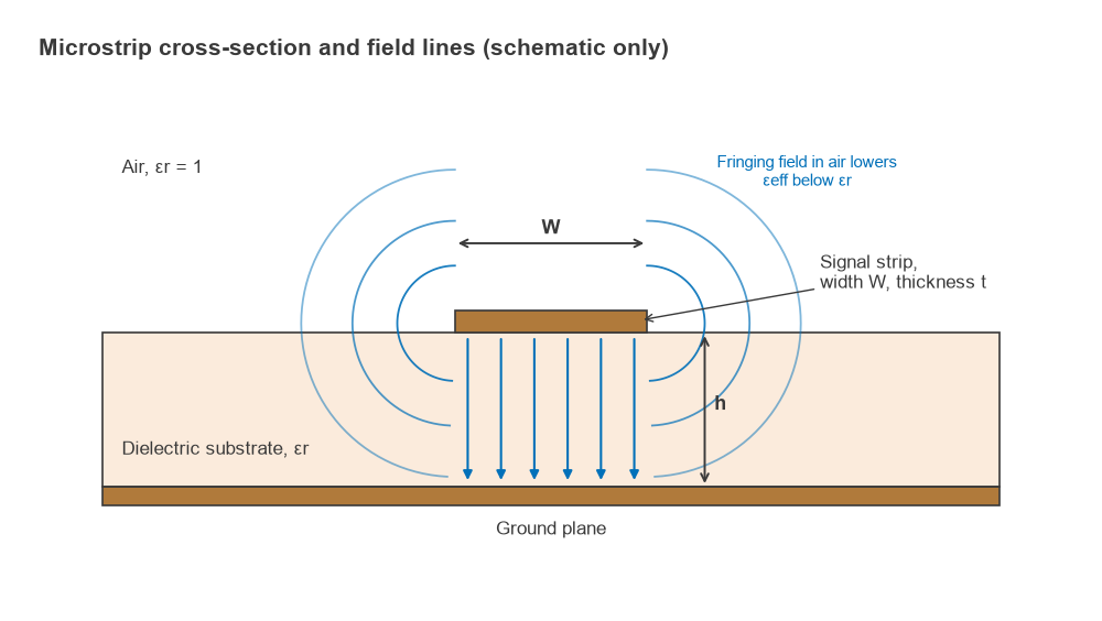
Once εeff is known, the other line properties follow directly. The phase velocity is vp = c/√εeff, the guided wavelength is λg = c/(f√εeff), and the delay per unit length is √εeff/c. Wider strips put more of the field in the substrate, so εeff rises toward εr and Z0 falls.
Effective Permittivity
The Hammerstad expressions for the static effective permittivity, with u = W/h, are
For u ≤ 1: εeff = (εr + 1)/2 + (εr − 1)/2 × [ (1 + 12/u)−1/2 + 0.04(1 − u)2 ]
For u ≥ 1: εeff = (εr + 1)/2 + (εr − 1)/2 × (1 + 12/u)−1/2
The first term, (εr + 1)/2, is the average of air and substrate, which is the limit for a very narrow strip. The second term pushes εeff toward εr as the strip widens.
Hammerstad and Wheeler Closed-Form Equations
With εeff in hand, the characteristic impedance for a strip of negligible thickness is
For u ≤ 1: Z0 = (60/√εeff) ln(8/u + u/4)
For u ≥ 1: Z0 = 120π / [ √εeff (u + 1.393 + 0.667 ln(u + 1.444)) ]
For design, the inverse problem is more useful: given Z0 and εr, find W/h. Wheeler’s synthesis equations, in the form given in most microwave textbooks, are
A = (Z0/60)√((εr + 1)/2) + ((εr − 1)/(εr + 1))(0.23 + 0.11/εr)
B = 377π / (2Z0√εr)
For W/h < 2: W/h = 8eA / (e2A − 2)
For W/h > 2: W/h = (2/π)[ B − 1 − ln(2B − 1) + ((εr − 1)/(2εr))(ln(B − 1) + 0.39 − 0.61/εr) ]
Accuracy
These simple forms are generally quoted as accurate to roughly 1 percent against full-wave solutions for zero-thickness strips over the usual range of W/h. The fuller Hammerstad and Jensen (1980) model, which includes strip thickness and a more elaborate εeff expression, is considerably more accurate and is what most commercial calculators implement. In practice the formula is rarely the largest error. The permittivity of a laminate can vary by several percent from its nominal value and with frequency, and finished copper and dielectric thicknesses carry their own tolerances. A 5 percent error in h moves Z0 by about 1.5 Ω on a 50 Ω line, far more than the difference between formula versions. Copper thickness t reduces Z0 slightly; a common correction widens the strip by ΔW = (t/π)(1 + ln(2h/t)), which for 35 µm copper on 1.6 mm FR-4 is about 0.06 mm. For final designs, especially at millimetre-wave frequencies, check the result with an EM field solver.
Worked Example: 50 Ω on 1.6 mm FR-4
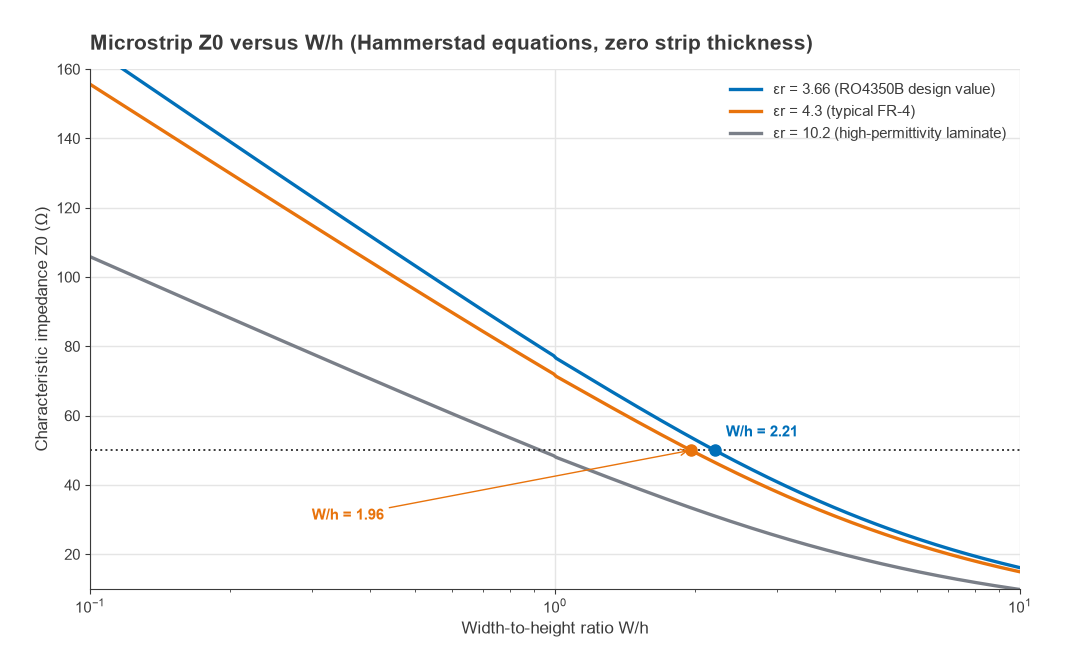
Design a 50 Ω line on a 1.6 mm board with εr = 4.3, a typical value for FR-4 near 1 GHz.
- Synthesis: A = (50/60)√(5.3/2) + (3.3/5.3)(0.23 + 0.11/4.3) = 1.357 + 0.159 = 1.516. Then W/h = 8e1.516/(e3.032 − 2) = 1.945, which is below 2, so the first formula applies. W = 1.945 × 1.6 = 3.11 mm.
- Check with the analysis equations: u = 1.945 gives εeff = 3.266 and Z0 = 50.2 Ω. Iterating the analysis equations to exactly 50.0 Ω gives W/h = 1.961, or W = 3.14 mm, with εeff = 3.268. The two methods agree within about 1 percent.
- Line properties: √εeff = 1.808, so the delay is 6.03 ps/mm and the static guided wavelength at 2.4 GHz is 69.1 mm, so a quarter-wave section is about 17.3 mm long. Including dispersion (next section) shortens the wavelength slightly, to about 68.7 mm.
- Thickness correction: with 35 µm copper the effective width grows by about 0.06 mm, so the drawn width for 50 Ω falls to roughly 3.08 mm.
A 3 mm trace on 1.6 mm FR-4 analyses to 51.4 Ω, which shows how forgiving the geometry is: a 0.14 mm change in width moves the impedance by only about 1.4 Ω.
50 Ω Width Table for Common Stackups
Because Z0 depends only on W/h and εr, the 50 Ω width scales linearly with substrate height. The table uses zero-thickness strips, εr = 4.3 for FR-4 and εr = 3.66 for RO4350B, which is approximately the manufacturer’s recommended design value for that laminate. Confirm both the permittivity and the finished thickness with the board fabricator before releasing a layout; the trade-offs between the two materials are covered in FR-4 vs Rogers.
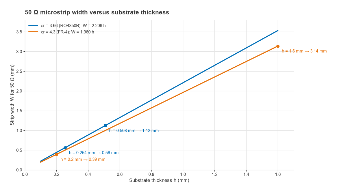
| Material | εr | h (mm) | W for 50 Ω (mm) | εeff |
|---|---|---|---|---|
| FR-4 (thin prepreg layer) | 4.3 | 0.20 | 0.39 | 3.27 |
| FR-4 | 4.3 | 0.36 | 0.71 | 3.27 |
| FR-4 | 4.3 | 0.80 | 1.57 | 3.27 |
| FR-4 | 4.3 | 1.60 | 3.14 | 3.27 |
| RO4350B | 3.66 | 0.254 | 0.56 | 2.85 |
| RO4350B | 3.66 | 0.508 | 1.12 | 2.85 |
| RO4350B | 3.66 | 0.762 | 1.68 | 2.85 |
| RO4350B | 3.66 | 1.524 | 3.36 | 2.85 |
The ratio W/h is 1.96 for FR-4 and 2.21 for RO4350B. On a multilayer board where the RF layer sits over a thin prepreg, the 50 Ω trace becomes narrow, which reduces the footprint mismatch at component pads but increases conductor loss. Transmission line losses explains how conductor and dielectric loss scale with width and frequency.
Microstrip Impedance Calculator
Enter the substrate and either a strip width (to analyse) or a target impedance (to synthesize). The calculator uses the Hammerstad equations above with the thickness correction, and estimates dispersion with the Getsinger model described in the next section. Results are first-pass design values, not a substitute for a field solver.
| Strip width W | – |
| Characteristic impedance Z0 | – |
| Static εeff | – |
| εeff at the entered frequency (Getsinger) | – |
| Guided wavelength λg at f | – |
| Delay | – |
| Transverse resonance estimate | – |
Dispersion and Frequency Limits
The quasi-TEM picture is a low-frequency approximation. As frequency rises, the field concentrates more in the substrate, so εeff increases from its static value toward εr. This is dispersion, and it lowers the phase velocity and raises the effective impedance seen by a resonator or filter designed with static values. A simple and widely used estimate is Getsinger’s model:
εeff(f) = εr − (εr − εeff(0)) / (1 + G(f/fp)2), with fp = Z0/(2μ0h) and G = 0.6 + 0.009Z0
For a 50 Ω line on 1.6 mm FR-4, fp = 12.4 GHz, and εeff rises from 3.27 at low frequency to about 3.42 at 5 GHz and 3.69 at 10 GHz. On 0.508 mm RO4350B, fp is 39 GHz, and εeff changes only from 2.85 to 2.91 over the same 10 GHz span. Thin substrates are much less dispersive, which is one reason high-frequency boards use them. More refined models, such as Kirschning and Jansen’s, are used in circuit simulators.
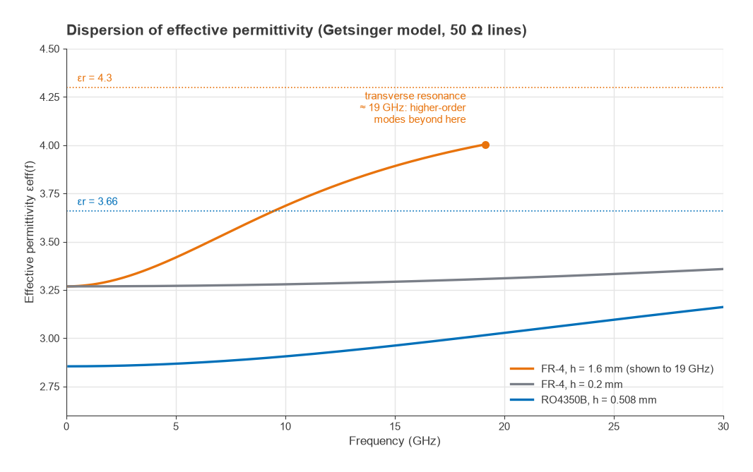
Two further limits set the useful upper frequency of a given microstrip. A wide strip can support a transverse resonance, a half-wave standing wave across its width, estimated at fc ≈ c / (√εr(2W + 0.8h)). For the 3.14 mm line on 1.6 mm FR-4 this is about 19 GHz. The substrate can also couple strongly to the lowest TM surface wave above roughly fT = c tan−1(εr) / (√2 πh√(εr − 1)), which is about 31 GHz for the same board. Designers usually keep the operating frequency well below both, which in practice means choosing a thinner substrate as frequency rises. Radiation from discontinuities and higher losses add further practical limits long before these mode boundaries are reached.
Microstrip vs Grounded Coplanar Waveguide
Grounded coplanar waveguide (GCPW) adds ground copper on the top layer on both sides of the strip, separated by a gap and stitched to the bottom ground with vias. The side grounds pull field out of the substrate and into the gaps, which reduces dispersion, improves isolation between neighbouring lines and gives a shorter ground return for shunt components. The cost is a narrower strip for the same impedance on a given board, more sensitivity to gap tolerance, and the need for a via fence. Microstrip remains simpler and is adequate for most work below a few gigahertz; coplanar waveguide and stripline take over where isolation, dispersion or shielding matter more.
Frequently asked questions
How do you calculate microstrip impedance?
Compute u = W/h, find εeff from the Hammerstad expression for the appropriate range of u, then apply the matching Z0 formula. For design, use Wheeler’s synthesis equations to get W/h from the target impedance and confirm the result with the analysis equations or a field solver.
What trace width is 50 ohm on FR-4?
With εr ≈ 4.3, a 50 Ω microstrip needs W ≈ 1.96h. That is about 3.1 mm on a 1.6 mm board and about 0.39 mm over a 0.2 mm dielectric. Because FR-4 permittivity varies between suppliers and with frequency, use the value from the laminate datasheet or the fabricator’s stackup.
Microstrip vs grounded coplanar waveguide?
Microstrip has one strip over a ground plane; GCPW adds top-side grounds and stitching vias next to the strip. GCPW gives lower dispersion and better isolation at higher frequencies, while microstrip is simpler, less sensitive to etch tolerance and adequate for most designs below a few gigahertz.
Does copper thickness change the impedance?
Yes, slightly. Thicker copper behaves like a wider strip and lowers Z0. For 35 µm copper on 1.6 mm FR-4 the effective width increase is about 0.06 mm, which lowers a 50 Ω line to about 49.4 Ω.
Related topics
The transmission line theory hub links the related line types. Wave propagation in transmission lines covers the underlying physics, microstrip filter design applies these lines to filters, and the impedance matching calculator and RF calculators collection offer related tools. Terms are defined in the wireless terms glossary.