

A PCB antenna is a radiating element etched from the copper of a printed circuit board, usually an inverted-F, meandered monopole or microstrip patch, that uses the board’s ground plane as part of its structure. Designing one means choosing a type that fits the space and bandwidth, sizing it to resonate at about a quarter or half of the effective wavelength, keeping a copper-free clearance around it, and finishing with a pi matching network tuned on the assembled board.
Printed antennas cost nothing beyond board area, which is why they appear in most Bluetooth, Wi-Fi, Zigbee and sub-GHz IoT products. They are also sensitive to everything around them. This page explains the main types, the geometry rules for the inverted-F and meander forms, the size limits set by physics, and a design flow that ends with tuning. It sits under the antennas hub of the RF design reference.
Types of PCB antenna
| Type | Resonant length | Strengths | Limitations |
|---|---|---|---|
| Printed monopole | about λeff/4 | Simple, wide bandwidth, near-omnidirectional | Long; needs a ground plane of comparable length |
| Inverted-F (IFA) | about λeff/4 (arm plus height) | Low profile along a board edge; feed impedance set by layout | Narrower bandwidth; sensitive to ground plane size |
| Meandered IFA (MIFA) or monopole | folded λeff/4 | Fits small areas | Lower efficiency and bandwidth as it shrinks |
| Microstrip patch | about λeff/2 | Directional, stable impedance, easy arrays | Large at low frequency; narrow bandwidth on thin substrates |
The inverted-F and its meandered form dominate 2.4 GHz consumer designs because they lie flat along one edge of the board. Patches suit higher frequencies, directional links and arrays, and are covered in depth on the patch antenna design page. Chip antennas and flexible printed antennas are alternatives when board area is scarce; practical notes on the flexible type are in integration tips for FPC antennas.
Inverted-F antenna geometry
An IFA starts as a quarter-wave monopole that has been bent over so that most of its length runs parallel to the ground plane edge. Bending it close to ground lowers the radiation resistance far below the monopole’s value, so a short circuit to ground is added near the bend and the feed is tapped a short distance S along from it. The result looks like the letter F lying on its side.
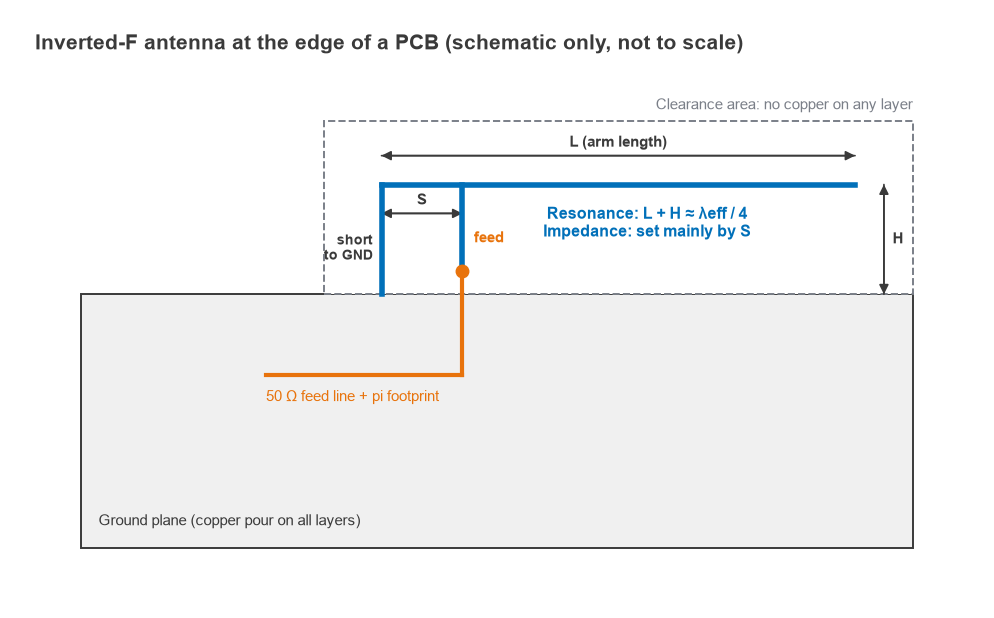
- Arm length L and height H. Their sum sets the resonant frequency: L + H ≈ λeff/4. Lengthening the arm lowers the frequency roughly in proportion.
- Feed-to-short spacing S. This mainly sets the input resistance. Moving the feed away from the short raises the resistance; moving it closer lowers it. It is the main layout control for reaching 50 Ω.
- Height H above the ground edge. A larger H raises radiation resistance and bandwidth but takes more board area.
- Trace width. Wider traces give slightly more bandwidth and lower conductor loss.
Estimating the resonant length
The effective wavelength depends on how much of the antenna’s field passes through the substrate. For a trace on the edge of a board, with air on one side and the laminate on the other, the effective permittivity lies between 1 (all air) and roughly (εr + 1)/2. At 2.45 GHz the free-space wavelength is 122.4 mm, so:
- εeff = 1 gives λ/4 = 30.6 mm
- εeff = (4.4 + 1)/2 = 2.7 for FR4 gives 30.6/√2.7 = 18.6 mm
- A mid-range estimate of εeff ≈ 1.9 gives 22.2 mm
The mid-range value is a sensible starting length for an EM simulation, not a final answer. Board thickness, the enclosure, the trace width and the ground plane shape all shift the result, which is why every printed antenna is tuned after it is built.
Ground plane and clearance rules
For an IFA or monopole, the ground plane is the other half of the antenna. Current flows along its edges, and much of the radiation comes from the ground plane itself, especially when the antenna element is electrically small. Several layout rules follow from this:
- Keep a clearance area under and around the antenna element free of copper on every layer, including inner planes. The reference design’s clearance dimensions should be copied exactly unless the antenna will be re-simulated.
- Place the antenna at a board edge, ideally a corner, so its field is not surrounded by ground.
- Give the ground plane enough length along the antenna’s axis. A ground plane much shorter than about a quarter wavelength reduces bandwidth and efficiency and shifts resonance.
- Stitch ground layers together with vias along the ground edge facing the antenna, as described in RF grounding and via stitching.
- Keep batteries, connectors, shield cans and screws out of the clearance and as far from the element as the mechanical design allows.
The feed line from the radio to the antenna should be a controlled 50 Ω trace, sized with the microstrip calculator or laid out as grounded coplanar waveguide. General layout practice is collected under RF PCB layout.
Meander antennas and the size limit
Folding the radiating arm into a meander packs a quarter wavelength of trace into less area. The penalty is that the antenna becomes electrically small, and small antennas have high Q and narrow bandwidth. The Chu limit gives the minimum Q of any antenna that fits inside a sphere of radius a:
Qmin = 1/(ka)3 + 1/(ka), where k = 2π/λ
For a matched antenna with Q, the largest fractional bandwidth within a VSWR of S is approximately (S − 1)/(Q√S). For S = 2, that is 1/(Q√2).
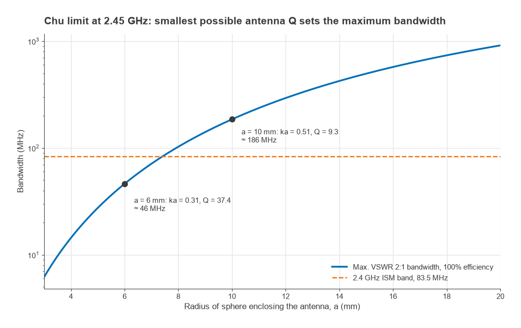
At 2.45 GHz, k = 0.0513 rad/mm. A structure that fits in a 10 mm radius sphere has ka = 0.51, Qmin = 9.3 and a maximum 2:1 bandwidth of 7.6%, or 186 MHz, comfortably wider than the 83.5 MHz ISM band. Shrinking to a 6 mm radius gives ka = 0.31, Qmin = 37.4 and only 46 MHz. That antenna cannot cover the whole band at a 2:1 VSWR even if it is lossless. Practical antennas fall short of the Chu bound, so real margins are smaller still.
There is an important qualification. Because the ground plane radiates, the sphere that matters encloses the significant ground currents, not only the printed element. A tiny meander on a large board can perform much better than its own dimensions suggest, and the same meander on a small module performs worse. The antenna parameters page explains how bandwidth, efficiency and gain are defined.
Patch antennas on PCB
A rectangular microstrip patch resonates when its length is about half a guided wavelength. The standard transmission-line model gives the width, effective permittivity, fringing extension and length:
W = (c/2f)√(2/(εr + 1))
εeff = (εr + 1)/2 + ((εr − 1)/2)(1 + 12h/W)−1/2
ΔL = 0.412h (εeff + 0.3)(W/h + 0.264) / ((εeff − 0.258)(W/h + 0.8))
L = c/(2f√εeff) − 2ΔL
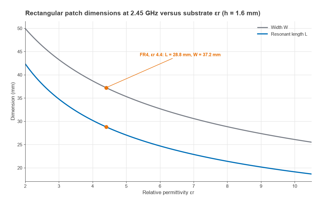
On 1.6 mm FR4 with εr = 4.4 at 2.45 GHz, these give W = 37.2 mm, εeff = 4.08, ΔL = 0.74 mm and L = 28.8 mm. That footprint is large for a handheld product, which is why patches at 2.4 GHz appear mainly in fixed equipment, and why they are more common at 5 GHz and above. FR4 loss also lowers patch efficiency; the trade-off between FR4 and low-loss laminates is discussed in FR4 vs Rogers.
Design flow for a PCB antenna
- Set the requirements: bands, return loss target, efficiency target, allowable area and board stack-up.
- Choose a type. Where possible, start from a published reference design for the same stack-up and copy it exactly, including clearance and ground plane size.
- Estimate the starting dimensions with the formulas above, then simulate the antenna together with the actual board outline and ground plane in a 3D field solver (see EM simulation basics).
- Add a pi matching footprint at the feed, populated with a 0 Ω series link by default.
- Build boards, assemble them into the enclosure and measure S11 at the feed with a calibrated VNA.
- If resonance is far off, trim or extend the arm. Then tune the residual mismatch with the pi network.
- Confirm radiated performance with an over-the-air or chamber measurement.
Tuning with a pi network: worked example
Suppose a first-build IFA with a combined arm length L + H of 24.0 mm resonates at 2.36 GHz in the enclosure. Since resonant frequency is roughly inversely proportional to length, the arm needs to shrink by the factor 2.36/2.45 = 0.963, to 23.1 mm. Trimming 0.9 mm from the open end of the arm moves the resonance close to 2.45 GHz.
After trimming, suppose the measured impedance at 2.45 GHz is 30 + j35 Ω. That gives |Γ| = 0.46, a return loss of only 6.7 dB. The admittance is 0.0141 − j0.0165 S. Its real part is below 1/50 S, so the first element from the antenna side is a shunt element that moves the admittance onto the r = 1 circle. Solving for the susceptance gives two options:
- Shunt capacitor 1.66 pF on the antenna side, then a series inductor of 2.10 nH (a low-pass network).
- Shunt capacitor 0.48 pF on the antenna side, then a series capacitor of 2.01 pF (a high-pass network).
The low-pass option uses more practical values and helps with harmonic suppression. Both use the antenna-side shunt position of the pi footprint and leave the radio-side shunt empty, which is exactly why the three-pad footprint is worth its board space. The complete measurement and tuning procedure, including fixture and cable effects, is on the antenna matching page, and the matching theory is covered in L-network matching and pi and T matching networks.
Frequently asked questions
How do you design a PCB antenna?
Pick a type that fits the available space, size it to about a quarter of the effective wavelength for an IFA or monopole, and keep a copper-free clearance around it. Simulate it with the real board outline, build it, measure S11 in the enclosure, then trim the arm and tune a pi matching network.
How long is a 2.4 GHz PCB antenna?
A free-space quarter wavelength at 2.45 GHz is 30.6 mm. Substrate loading shortens a printed element, so an inverted-F on FR4 usually ends up somewhere between about 19 mm and 30 mm of total length, depending on stack-up and layout. Simulation and measurement set the final value.
Why does a PCB antenna need a ground plane?
Monopole-type antennas, including the IFA, work against an image in the ground plane, and currents on the ground plane radiate. If the ground plane is too small or badly shaped, the antenna’s resonance, bandwidth and efficiency all suffer.
Can a PCB antenna be made smaller without loss?
Not indefinitely. The Chu limit ties the minimum Q, and so the maximum bandwidth, to the antenna’s electrical size. Meandering and loading can shrink an antenna, but bandwidth and usually efficiency fall as it gets smaller.
Related topics
See antenna parameters for definitions of gain and efficiency, patch antenna design for the half-wave alternative, and antenna matching for in-product tuning. The system view of antennas in a radio is covered in antennas and propagation in radio design, and coexistence between several antennas on one board in RF coexistence. Terms are defined in the wireless terms glossary.