

Grounding is critical in RF because every signal current returns through the ground structure. At high frequency that return current flows directly under the signal path and sees inductance, not just resistance. A ground that is broken, split or connected through long vias adds impedance, shifts matching, couples circuits together and radiates. Via stitching and continuous reference planes keep the return path short and predictable.
This page is part of the RF PCB layout section of the RF design guide. It covers how return current behaves, why split planes cause trouble, how to estimate via inductance, and how to place stitching vias and ground fences on a real board.
Where RF return current actually flows
At DC, return current spreads across a ground plane along the path of least resistance. As frequency rises into the tens and hundreds of kilohertz the picture changes: the current takes the path of least inductance, which is the path that minimises the loop area between the forward and return currents. For a trace over a plane, that path lies directly underneath the trace.
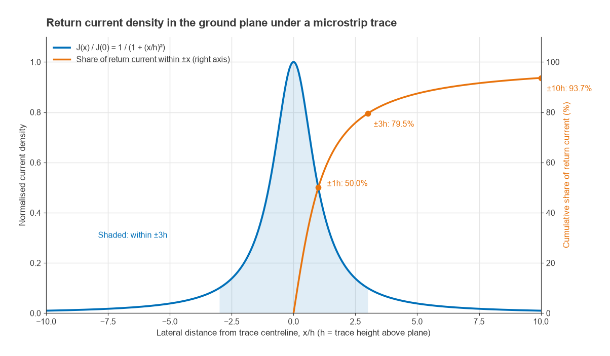
For a thin microstrip at height h above an infinite plane, the return current density across the plane follows a simple approximate distribution:
J(x) = (I / πh) × 1 / (1 + (x/h)2)
where x is the lateral distance from the trace centreline. Integrating gives the share of return current within ±x of the trace: (2/π)·arctan(x/h). Half the current flows within ±1h, 79.5% within ±3h, and 93.7% within ±10h. On a four-layer board with 0.2 mm between the top layer and the layer-2 ground, 80% of the return current for a top-layer trace is confined to a strip about 1.2 mm wide.
The practical consequence is that the ground directly under and beside every RF trace is part of the transmission line. The characteristic impedance a microstrip calculator reports assumes that ground is continuous. Anything that interrupts it changes the line.
Split-plane hazards
A slot, gap or split in the reference plane under a trace forces the return current to detour around it. The detour enlarges the current loop, which adds series inductance to the line, creates a local impedance discontinuity and turns the slot into an antenna. A slot of length λ/2 resonates and can radiate efficiently. At 2.4 GHz on an FR-4 board that is only about 30 to 40 mm, depending on how much of the field is in the dielectric.
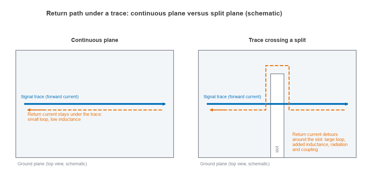
Common causes include:
- Separate “analog” and “digital” ground pours with a gap between them that a trace crosses.
- A row of closely spaced vias or antipads that perforates the plane into a slot.
- Power-plane splits on the reference layer for traces routed on an adjacent layer.
- A trace changing layers without a nearby ground via, so the return current has no path between reference planes.
For most mixed-signal RF boards the safer approach is a single, unbroken ground plane with careful component placement, so that noisy and sensitive circuits are separated by distance rather than by cuts. Where a split is unavoidable, no trace should cross it, and a stitching capacitor or bridge should give the return current a path at the crossing point. Interference between circuits on one board is covered further under RF coexistence and EMC and EMI.
Via inductance
A via that connects a component pad or a top-layer ground pour to an inner plane is a short length of wire, and its inductance is often the largest parasitic in an RF ground connection. A widely used closed-form estimate for a cylindrical via of height h and radius r is the Goldfarb–Pucel expression:
L = (μ0 / 2π) × [ h·ln((h + √(r2 + h2)) / r) + 1.5(r − √(r2 + h2)) ]
with μ0/2π = 2 × 10⁻⁷ H/m. A simpler rule of thumb, L ≈ 0.2h[ln(4h/d) + 1] nH with h and diameter d in millimetres, is also common. It gives values about twice as high for typical board vias, so it is best treated as a pessimistic upper estimate. Neither formula includes pad, antipad or plane-spreading effects, so EM simulation is the reference when a via is part of a matching network. The broader topic of package and board parasitics is covered in RF component parasitics.
Worked example: grounding a shunt capacitor at 2.4 GHz
Take a 0.3 mm drilled via through a 1.6 mm two-layer board, so h = 1.6 mm and r = 0.15 mm.
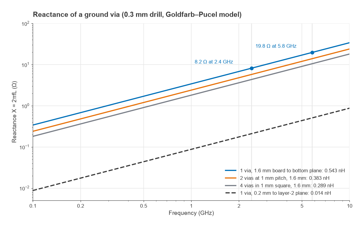
- √(r2 + h2) = 1.607 mm, and ln((1.6 + 1.607) / 0.15) = ln(21.38) = 3.062.
- The bracket is 1.6 × 3.062 + 1.5 × (0.15 − 1.607) = 4.899 − 2.185 = 2.714 mm.
- L = 2 × 10−7 × 2.714 × 10−3 = 0.543 nH.
- At 2.4 GHz, XL = 2π × 2.4 × 109 × 0.543 × 10−9 = 8.2 Ω. At 5.8 GHz it is 19.8 Ω.
Now place a 10 pF capacitor from an RF node to ground through that via. The capacitor’s reactance at 2.4 GHz is 1 / (2π × 2.4 × 109 × 10 × 10−12) = 6.6 Ω, smaller than the via’s 8.2 Ω. The series resonance of the via inductance with 10 pF is 1 / (2π√(0.543 nH × 10 pF)) = 2.16 GHz, before even counting the capacitor’s own ESL. At 2.4 GHz this “short to ground” is already inductive.
Two remedies are available. Moving the ground plane closer helps most: on a four-layer board with the plane 0.2 mm below the top layer, the same formula gives about 0.014 nH and 0.21 Ω at 2.4 GHz. Paralleling vias also helps, but less than 1/N because closely spaced vias share magnetic flux. Using the partial mutual inductance of two parallel 1.6 mm conductors, two vias at 1 mm pitch give about 0.383 nH (5.8 Ω at 2.4 GHz), not 0.27 nH. Four vias in a 1 mm square give about 0.289 nH (4.4 Ω).
The same inductance sits in the source or emitter lead of an amplifier transistor, where it acts as degeneration, reduces gain and can change stability. Designers of low-noise amplifiers either minimise it or include it deliberately in the input match.
Via stitching and ground fences
Stitching vias tie top-layer ground pour to the inner and bottom planes at regular intervals. They serve three purposes: they hold the copper pours at the same potential so they do not float and resonate, they suppress parallel-plate modes between planes, and, placed in rows, they form fences that confine fields around a trace or a circuit block.
Choosing the via pitch
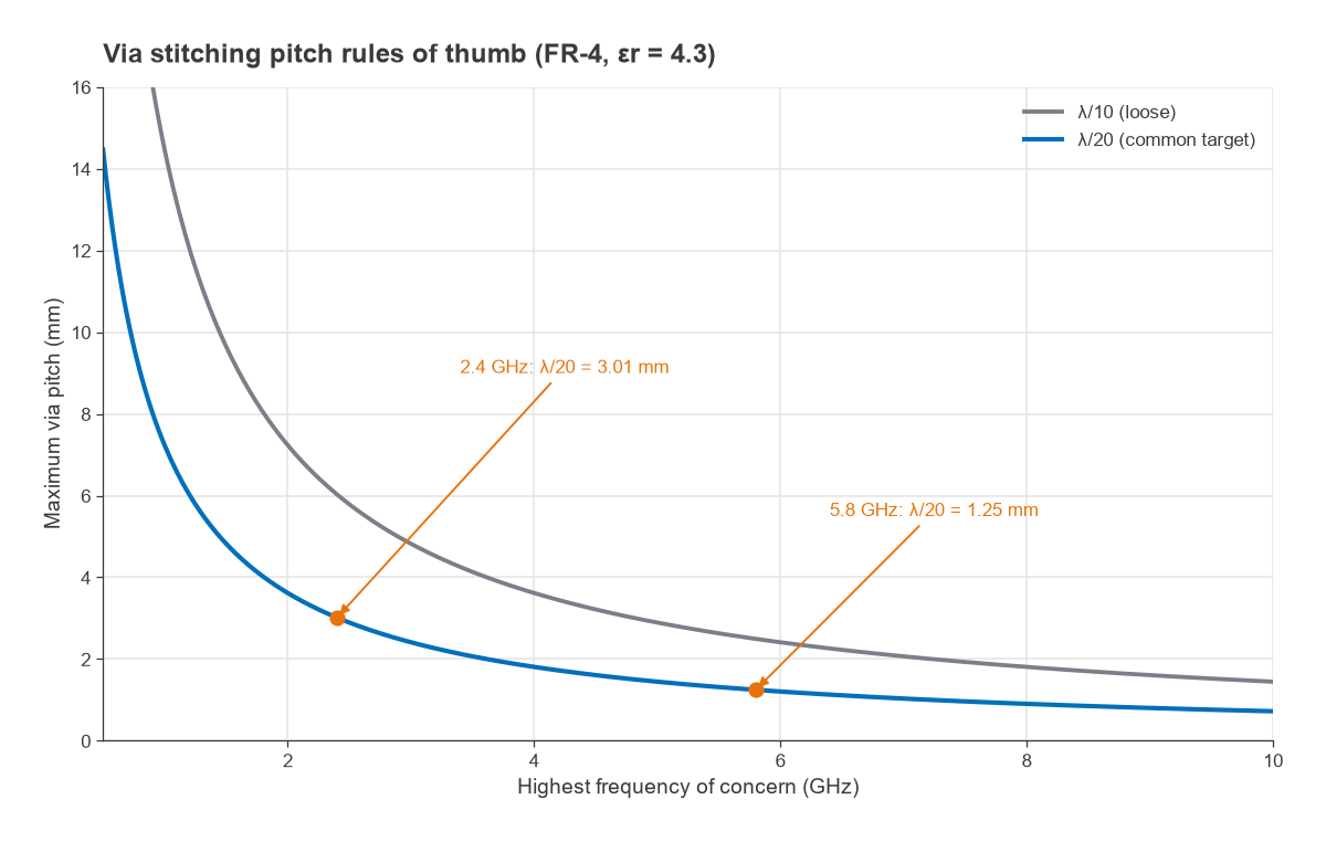
The usual guideline is a via pitch of no more than λ/10 to λ/20 at the highest frequency of concern, where λ is the wavelength in the dielectric. Using the bulk permittivity gives a conservative answer:
λ = c / (f √εr)
| Frequency | λ in FR-4 (εr = 4.3) | λ/10 | λ/20 |
|---|---|---|---|
| 1 GHz | 144.7 mm | 14.5 mm | 7.2 mm |
| 2.4 GHz | 60.3 mm | 6.0 mm | 3.0 mm |
| 5.8 GHz | 24.9 mm | 2.5 mm | 1.25 mm |
| 10 GHz | 14.5 mm | 1.45 mm | 0.72 mm |
The frequency of concern is not just the operating frequency. Harmonics of a power amplifier, a crystal or a fast digital clock often set it. A 2.4 GHz transmitter whose third harmonic at 7.2 GHz must be kept off the board edge needs denser stitching than the fundamental alone suggests.
Fences along transmission lines
Grounded coplanar waveguide needs a row of vias along both side grounds, close to the gap, to keep the top grounds tied to the bottom plane and prevent unwanted modes. The same idea applies to microstrip routed near other traces: a fenced ground strip between two lines usually isolates them much better than the same bare spacing. Fences are also the base of a shield can footprint, where the can’s wall pads need dense stitching to make the can a continuous enclosure.
Step-by-step grounding checklist
- Choose a stack-up with a solid ground plane directly under every RF layer. The trade-offs between laminates and layer counts are covered in FR-4 vs Rogers.
- Keep the plane under RF traces unbroken. Route nothing on the plane layer in the RF area.
- Give every grounded RF component pad its own via or vias, placed inside or immediately next to the pad.
- Estimate via inductance at the operating frequency and include it in matching and decoupling calculations.
- Place a ground via within about one line width of every signal via that changes reference planes.
- Stitch ground pours at λ/20 or tighter at the highest frequency of concern, and fence board edges and RF lines.
- Remove isolated copper islands, or stitch them to ground, so they cannot resonate.
Supply decoupling relies on the same low-inductance ground, and the capacitor selection side of that problem is covered in power supply decoupling for RF circuits.
Frequently asked questions
Why is grounding critical in RF?
Ground is the return half of every RF circuit. At high frequency the return current follows the signal path closely, and any inductance or discontinuity in that path changes impedances, couples signals between circuits and causes radiation. A low-inductance, continuous ground keeps the circuit behaving as designed.
How far apart should stitching vias be?
A common rule is no more than λ/20 at the highest frequency of concern, using the wavelength in the dielectric. In FR-4 that is about 3 mm at 2.4 GHz and 1.25 mm at 5.8 GHz. A pitch of λ/10 is sometimes accepted where space is tight and the frequency content is well controlled.
Should RF and digital grounds be separated?
On most RF boards, no. A single continuous plane with good placement usually performs better than split grounds, because a split creates slot antennas and long return detours. Separation by distance, routing discipline and shielding is generally more effective than cutting the plane.
How much inductance does a via have?
A 0.3 mm via through a 1.6 mm board is roughly 0.5 nH by the Goldfarb–Pucel estimate, which is 8 Ω of reactance at 2.4 GHz. A via to a plane only 0.2 mm away is a few hundredths of a nanohenry or less. Pads and antipads add to these figures.
Related topics
The transmission line theory behind return paths is introduced in transmission line theory, and the impedance effects of discontinuities in VSWR and return loss. Terms used on this page are defined in the wireless terms glossary.