

Pi and T matching networks are three-element lumped matching circuits that let the designer choose the network Q, and therefore the bandwidth, instead of accepting the fixed Q of a two-element L-network. Use a pi or T instead of an L when you need a narrower bandwidth, more harmonic suppression, or component values that are easier to build. The usual design method splits the network into two L-sections that meet at an imaginary “virtual resistance”.
Pi and T networks build directly on the L-network, and both belong to the broader topic of impedance matching. This page shows how to design them step by step, how to pick Q, and why a low-pass pi is the classic output network for power amplifiers.
Why add a third element
An L-network matching Rlow to Rhigh has exactly one Q for each topology:
QL = √(Rhigh/Rlow − 1)
That Q sets the bandwidth, the harmonic attenuation and the component values together. A 4:1 ratio gives Q = 1.73, which is broadband but provides little filtering. A third element adds one degree of freedom, so Q can be set anywhere above the L-network minimum. The pi network has a shunt element at each port and one series element in the middle; the T network is the dual, with a series element at each port and one shunt element in the middle.
The virtual resistance method
A pi or T network can be viewed as two L-networks connected back to back. The first L transforms one port to an intermediate resistance Rv, and the second transforms Rv to the other port. Rv never appears as a physical resistor; it is the resistance seen at the junction between the two halves.
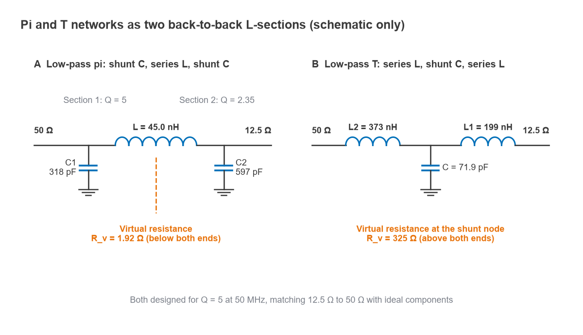
- Pi network: each L has its shunt element at the outer port and its series element facing the middle, so Rv must be lower than both terminating resistances. For a chosen Q on the higher-resistance side, Rv = Rhigh/(Q2 + 1).
- T network: each L has its series element at the outer port and its shunt element in the middle, so Rv must be higher than both. For a chosen Q on the lower-resistance side, Rv = Rlow(Q2 + 1).
The network Q is normally taken as the higher of the two section Qs. That is the section that dominates the bandwidth, and it is the one the designer specifies.
Design steps for a pi network
- Choose the loaded Q. It must exceed the L-network value √(Rhigh/Rlow − 1).
- Compute Rv = Rhigh/(Q2 + 1).
- High side: shunt reactance Xp1 = Rhigh/Q and series reactance Xs1 = Q × Rv.
- Low side: Q2 = √(Rlow/Rv − 1), shunt reactance Xp2 = Rlow/Q2 and series reactance Xs2 = Q2 × Rv.
- Combine the two series reactances into one element: Xs = Xs1 + Xs2 if they are the same type.
- Convert to component values with L = X/(2πf) and C = 1/(2πfX), then simulate with real parts.
The T network follows the same steps with the roles reversed: series reactances Xs = Q × R at each outer port, shunt reactances Rv/Q in the middle, and the two shunt elements combined in parallel.
Worked example: 12.5 Ω to 50 Ω at 50 MHz
Suppose a transistor stage needs a 12.5 Ω load at 50 MHz and the output must drive a 50 Ω system. The L-network Q would be √(50/12.5 − 1) = 1.73. Choose a low-pass pi with Q = 5 for more selectivity.
- Rv = 50/(52 + 1) = 50/26 = 1.923 Ω.
- 50 Ω side: Xp1 = 50/5 = 10.0 Ω, so C1 = 1/(2π × 50 MHz × 10.0) = 318 pF. Xs1 = 5 × 1.923 = 9.62 Ω.
- 12.5 Ω side: Q2 = √(12.5/1.923 − 1) = √5.5 = 2.345. Xp2 = 12.5/2.345 = 5.33 Ω, so C2 = 597 pF. Xs2 = 2.345 × 1.923 = 4.51 Ω.
- Series inductor: Xs = 9.62 + 4.51 = 14.13 Ω, so L = 14.13/(2π × 50 MHz) = 45.0 nH.
For the T version at the same Q, Rv = 12.5 × 26 = 325 Ω. The 12.5 Ω side needs a series reactance of 5 × 12.5 = 62.5 Ω (199 nH) and a shunt reactance of 325/5 = 65.0 Ω. The 50 Ω side has Q2 = √(325/50 − 1) = 2.345, a series reactance of 117.3 Ω (373 nH) and a shunt reactance of 138.6 Ω. The two shunt reactances in parallel give 44.2 Ω, a single 71.9 pF capacitor.
| Network (12.5 Ω to 50 Ω, 50 MHz) | Components | −20 dB return-loss band | |S21| at 100 MHz | |S21| at 150 MHz |
|---|---|---|---|---|
| Low-pass L, Q = 1.73 | Shunt 110 pF, series 68.9 nH | 46.53 to 53.24 MHz (13.4%) | −7.8 dB | −15.7 dB |
| Low-pass pi, Q = 3 | 191 pF, 67.2 nH, 312 pF | 48.48 to 51.40 MHz (5.8%) | −19.7 dB | −31.5 dB |
| Low-pass pi, Q = 5 | 318 pF, 45.0 nH, 597 pF | 49.24 to 50.72 MHz (3.0%) | −26.0 dB | −38.0 dB |
| Low-pass pi, Q = 10 | 637 pF, 23.5 nH, 1254 pF | 49.65 to 50.34 MHz (1.4%) | −32.8 dB | −44.8 dB |
| Low-pass T, Q = 5 | 373 nH, 71.9 pF, 199 nH | 49.24 to 50.72 MHz (3.0%) | −26.0 dB | −38.0 dB |
All figures in the table come from a circuit simulation of ideal components, with the input referenced to 50 Ω and the output terminated in 12.5 Ω. The low-pass pi and low-pass T at the same Q are duals and give identical responses here; the choice between them is about practical component values and DC paths.
Choosing Q: bandwidth and loss
Bandwidth falls roughly in proportion to 1/Q. In the example, raising Q from the L-network minimum of 1.73 to 3, 5 and 10 shrinks the 20 dB return-loss bandwidth from 13.4% to 5.8%, 3.0% and 1.4%. A narrow match is useful when the network must also filter, and harmful when the system has to tolerate component tolerances or cover a band.
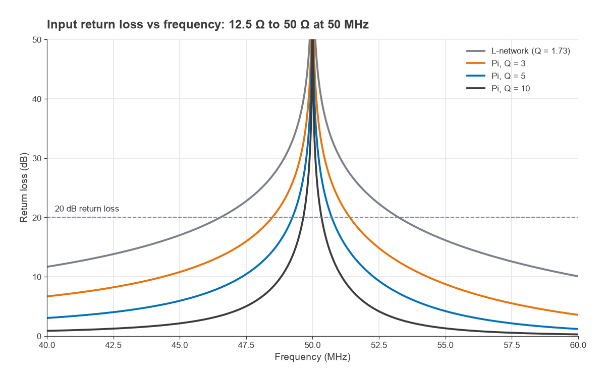
Loss grows with Q because circulating currents grow with Q. For small losses the insertion loss of a pi network is approximately
IL ≈ 4.34 (Q1 + Q2)(1/Qu,L + 1/Qu,C) dB
where Qu is the unloaded Q of the inductors and capacitors. With an inductor Qu of 100 and capacitor Qu of 500, the estimate gives 0.22 dB at Q = 3, 0.38 dB at Q = 5 and 0.78 dB at Q = 10, against 0.09 dB for the L-network. A simulation with the same lossy parts gives 0.22, 0.38 and 0.75 dB. At a power amplifier output, 0.38 dB is about 8% of the output power turned into heat in the matching network, which is why designers rarely push Q higher than the harmonic or bandwidth requirement demands. The Q-factor page covers unloaded and loaded Q in more depth.
Practical guidance for a first design: start with Q between about 1.5 and 3 times the L-network minimum, then adjust to meet the harmonic and bandwidth requirements. Very high Q also makes the match sensitive to component tolerance, because a few percent change in a reactance moves the resonance by a significant fraction of the bandwidth.
Harmonic suppression of pi networks
A low-pass pi is a third-order low-pass filter. Above the design frequency, the series inductor’s reactance rises while both shunt capacitors’ reactances fall, so attenuation rises at about 18 dB per octave well above resonance. An L-network is only second order, with about 12 dB per octave. Figure 3 shows the effect for the 50 MHz example: at the second harmonic the Q = 5 pi attenuates by 26.0 dB against 7.8 dB for the L-network, and at the third harmonic by 38.0 dB against 15.7 dB.
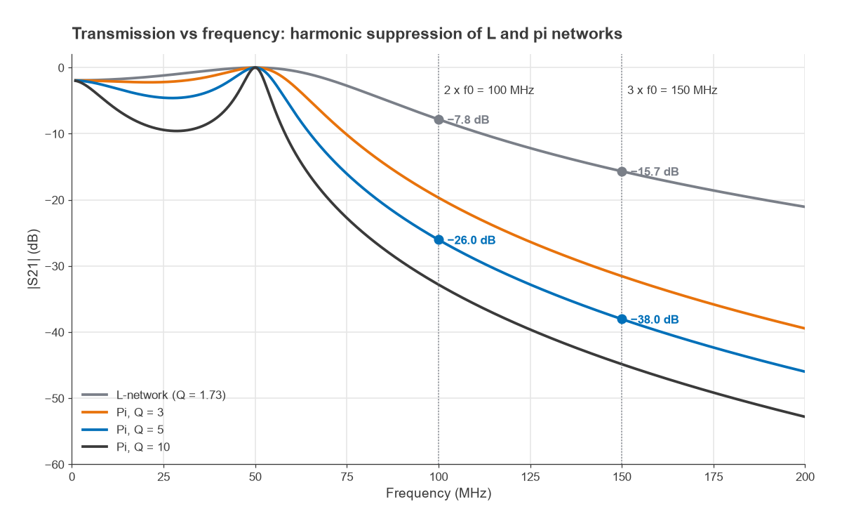
That is why the pi network has been the standard tank and output network for transmitters for most of radio history. It matches the device, filters its harmonics, and puts a capacitor across each port, which conveniently absorbs the output capacitance of the transistor or tube on one side and gives a low-impedance shunt path for harmonics on the other. A high-pass pi or T (series capacitors, shunt inductors) attenuates below the design frequency instead, which suits interstage matching where low-frequency gain must be suppressed or where the shunt inductors double as bias feeds.
Harmonic attenuation from a single matching network is rarely enough to meet a spurious-emission limit on its own, which is typically tens of decibels below the carrier. A separate low-pass filter usually follows; see LC filter design for the method.
Pi or T: practical selection
- Absorbing device capacitance: a pi with shunt capacitors at the ports absorbs the output capacitance of a transistor or the input capacitance of the next stage. A T with series inductors absorbs series lead and package inductance.
- Component values: a pi between low resistances tends to need large capacitors and a small inductor, as the 597 pF and 45 nH in the example show. A T between the same resistances needs larger inductors and a small capacitor. Pick the version whose values are realizable with good Q at the frequency.
- DC paths: low-pass forms pass DC through the series element; high-pass forms block it. Choose according to how bias is fed.
- Parasitics: at high frequencies, pad capacitance favours shunt capacitors at the ports, and the pi often maps more naturally onto a printed layout.
At microwave frequencies the same ideas carry over to distributed circuits: the quarter-wave transformer and stub matching replace lumped parts with line sections, and the Smith chart shows a pi network as two L-network paths meeting at the constant-Q contour chosen by the designer.
Frequently asked questions
When use a pi network instead of an L?
Use a pi when the L-network’s fixed Q gives too much bandwidth or too little harmonic suppression, or when its component values are impractical. A pi lets you set Q above the L-network minimum and adds a third pole of low-pass filtering.
What is the virtual resistance in a pi network?
It is the intermediate resistance where the two back-to-back L-sections meet. For a pi it is lower than both port resistances and equals Rhigh/(Q2 + 1); for a T it is higher than both and equals Rlow(Q2 + 1).
What Q should I choose for a pi matching network?
Choose the lowest Q that meets the harmonic and selectivity requirements. Higher Q narrows bandwidth, raises loss and increases sensitivity to component tolerances. A starting point of 1.5 to 3 times the L-network Q is common.
Related topics
The L-network page explains the two-element building block, and broadband matching covers the opposite goal of minimum Q over a wide band. Component values can be checked with the impedance matching calculator, and PA output networks are discussed under power amplifier classes. For the wider context see RF design and the wireless terms glossary.