

An L-network is the simplest lossless impedance matching network: two reactive elements, one in series and one in shunt, arranged in the shape of the letter L. To design one between two resistances, compute Q = √(Rhigh/Rlow − 1), make the series reactance Q × Rlow and the shunt reactance Rhigh/Q, and place the shunt element across the higher resistance. Choosing an inductor or a capacitor for each position gives a low-pass or a high-pass version.
The L-network is the building block of most lumped matching in RF circuits, and the starting point for the pi and T networks that add a third element to control bandwidth. It sits under impedance matching in the RF design map.
How an L-Network Transforms Impedance
The L-network works through a series-to-parallel conversion. A resistance Rs in series with a reactance Xs has a quality factor Q = Xs/Rs. At a single frequency, that series combination is exactly equivalent to a larger resistance Rp in parallel with a reactance Xp, where
Rp = Rs(1 + Q2), Xp = Xs(1 + Q2)/Q2
So adding series reactance to a small resistance makes it look, in parallel form, like a larger resistance with some parallel reactance attached. If the shunt element of the L cancels that parallel reactance, only Rp remains. Setting Rp equal to the higher resistance fixes Q, and from Q both reactances follow. The same Q appears in both branches, which is why it is called the network’s Q. The Q-factor page covers the series-parallel equivalence in more depth.
Design Equations
For matching a resistance Rlow to a resistance Rhigh:
- Network Q: Q = √(Rhigh/Rlow − 1)
- Series reactance, next to Rlow: |Xs| = Q × Rlow
- Shunt reactance, across Rhigh: |Xp| = Rhigh/Q
- Component values: L = X/(2πf), C = 1/(2πfX)
The two reactances must be of opposite type: if the series element is an inductor, the shunt element is a capacitor, and the other way round. Q is fixed by the resistance ratio. This is the L-network’s main limitation: the designer cannot choose its bandwidth independently, because there is only one solution for each topology.
Design steps
- Identify Rhigh and Rlow at the design frequency. If the load is complex, note its reactance.
- Compute Q from the resistance ratio.
- Choose low-pass (series L, shunt C) or high-pass (series C, shunt L) based on harmonic filtering, DC path and bias needs.
- Compute the series and shunt reactances; adjust the series reactance to absorb or cancel any load reactance.
- Convert to component values, pick the nearest standard parts, and simulate including parasitics and pad layout.
The Four Topologies
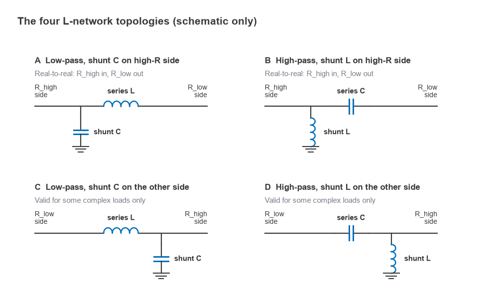
Two choices define an L-network: which element type sits in series, and on which side the shunt element sits. That gives four arrangements. For a match between two pure resistances, only the two with the shunt element across the higher resistance work:
- Low-pass: series inductor, shunt capacitor. It passes DC through the series path and attenuates harmonics, which makes it the usual choice at the output of a power amplifier.
- High-pass: series capacitor, shunt inductor. It blocks DC through the series capacitor and gives a DC path to ground through the shunt inductor, which can double as a bias feed or an ESD path.
The other two arrangements put the shunt element across the lower resistance. They cannot match two pure resistances, but with a complex load they become valid whenever the load’s admittance already lies inside the unit-conductance circle of the Smith chart. In general, a complex load has at most two working L-network solutions out of the four topologies, and which two depends on where the load sits on the chart. A load whose real part already equals the source resistance needs only a single series element, and one whose conductance already matches needs only a shunt element.
Worked Example: 50 Ω to 10 Ω at 2.4 GHz
Match a 10 Ω resistive load, typical of a small power transistor’s optimum load, to a 50 Ω system at 2.4 GHz.
- Q = √(50/10 − 1) = √4 = 2.
- Series reactance at the 10 Ω side: Xs = 2 × 10 = 20 Ω.
- Shunt reactance across the 50 Ω side: Xp = 50/2 = 25 Ω.
| Topology | Series element (20 Ω) | Shunt element (25 Ω) |
|---|---|---|
| Low-pass | L = 20 / (2π × 2.4 GHz) = 1.33 nH | C = 1 / (2π × 2.4 GHz × 25) = 2.65 pF |
| High-pass | C = 1 / (2π × 2.4 GHz × 20) = 3.32 pF | L = 25 / (2π × 2.4 GHz) = 1.66 nH |
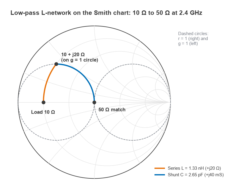
Check the low-pass version. The series inductor turns the 10 Ω load into 10 + j20 Ω. Its admittance is 1/(10 + j20) = 0.02 − j0.04 S. The real part, 0.02 S, is exactly 1/50 Ω. The shunt capacitor adds +j0.04 S, cancelling the imaginary part and leaving 0.02 S, which is 50 Ω. On a Smith chart the series inductor moves the load up a constant-resistance circle until it meets the unit-conductance circle, and the shunt capacitor then moves it along that circle to the centre.
Values this small are sensitive to layout. A 1.33 nH inductor is comparable to the inductance of a few millimetres of narrow trace or of a component’s pads and vias, so in practice part of the series inductance is often realized as a short length of high-impedance microstrip, and the whole network is tuned in simulation with real component parasitics and self-resonance included.
Absorbing load reactance
Suppose the load is 10 − j5 Ω instead of a pure 10 Ω. The low-pass network still needs the load plus series element to total 10 + j20 Ω, so the series inductor must supply +j25 Ω instead of +j20 Ω. That is 1.66 nH. The load’s capacitance has been absorbed into the network rather than cancelled separately. Absorption works whenever the load reactance has the opposite sign to the required series reactance or is smaller than it; otherwise the excess must be resonated out first, which costs bandwidth.
Bandwidth and Q
An L-network is a resonant circuit, so its bandwidth falls as its Q rises. Because Q is set by the resistance ratio, larger transformation ratios mean narrower matches: a 2:1 ratio gives Q = 1, 5:1 gives Q = 2, 10:1 gives Q = 3, and 20:1 gives Q ≈ 4.4. When both ends are terminated, the loaded Q of the circuit is roughly half the network Q, and the fractional bandwidth is roughly inversely proportional to Q.
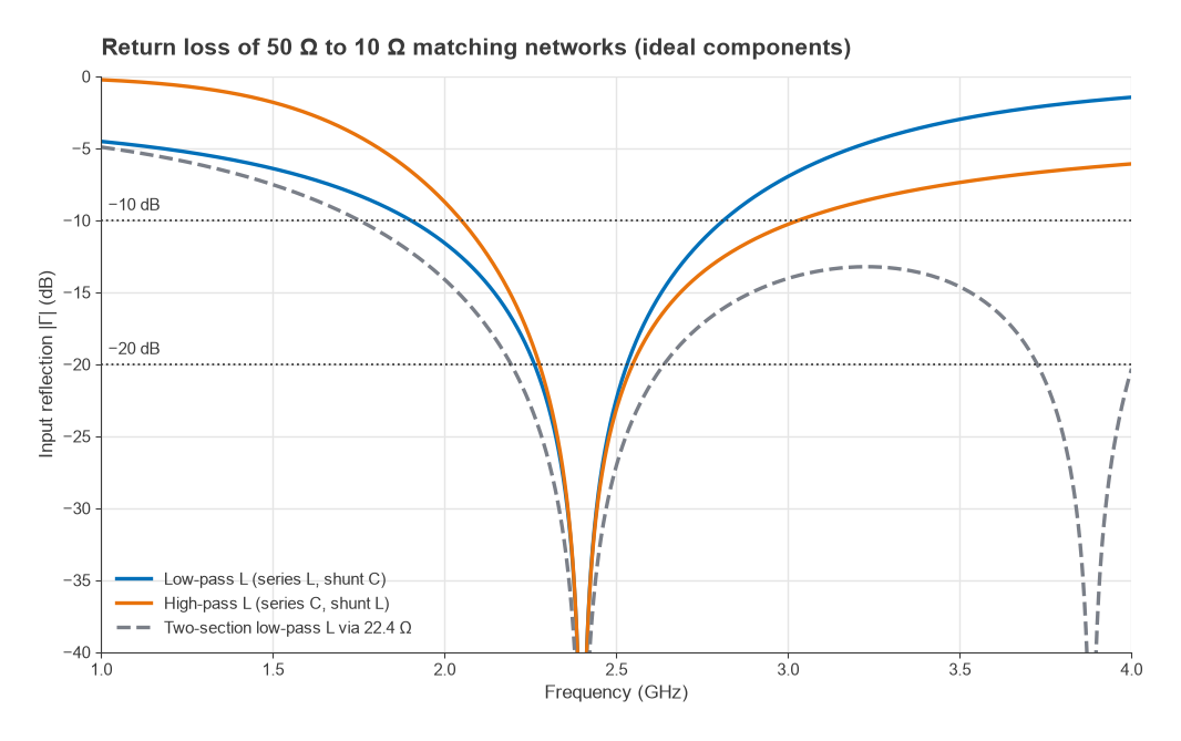
For the 2.4 GHz example with ideal components, the low-pass version keeps the input reflection below −20 dB (a return loss of 20 dB, VSWR about 1.22) from 2.26 to 2.53 GHz, a fractional bandwidth of 11.3%. The −10 dB band runs from 1.90 to 2.81 GHz, about 38%. The high-pass version has almost the same −20 dB bandwidth, 11.3%, but its response is skewed toward higher frequencies. VSWR and return loss explains how these figures convert.
To widen the match, split the transformation into steps of lower Q. Two L-sections in cascade, first from 10 Ω to the geometric mean √(10 × 50) = 22.4 Ω and then from 22.4 Ω to 50 Ω, each have Q = √(50/22.4 − 1) = 1.11. With ideal parts the −20 dB bandwidth grows to about 18.6%, from 2.19 to 2.64 GHz, and the −10 dB bandwidth extends from 1.75 GHz to above 4 GHz. More sections continue the trend toward the limits described in broadband matching. To narrow the match deliberately, for example to add selectivity, a pi or T network raises Q above the L-network’s minimum.
Losses and Component Q
Real inductors and capacitors have finite unloaded Q, Qu. For a single L-network, the fraction of power lost is approximately Q/Qu for each element, so the insertion loss in decibels is roughly 4.34 × Q × (1/QL,u + 1/QC,u) for small losses. With Q = 2 and an inductor Qu of 40 and a capacitor Qu of 200, the estimate is 4.34 × 2 × (0.025 + 0.005) = 0.26 dB. Higher transformation ratios cost more loss for the same parts, which is another reason to split large ratios into several sections and to use high-Q inductors in the series position, where the current is highest.
Frequently asked questions
How do you design an L matching network?
Compute Q = √(Rhigh/Rlow − 1). Put a series reactance of Q × Rlow next to the lower resistance and a shunt reactance of Rhigh/Q across the higher resistance, using opposite element types. Convert the reactances to inductance and capacitance at the design frequency.
How many L-network solutions exist?
There are four L topologies. Between two pure resistances, two of them work: the low-pass and the high-pass forms with the shunt element across the higher resistance. For a complex load, at most two of the four work, and which ones depends on where the load lies on the Smith chart.
Why is the bandwidth of an L-network fixed?
With only two elements, both reactances are fixed by the resistance ratio, so Q is fixed as well. Adding a third element (pi or T) or cascading sections gives the extra degree of freedom needed to set bandwidth.
Should I use a low-pass or high-pass L-network?
Use low-pass when harmonic suppression or a DC path through the series element is wanted, as at a PA output. Use high-pass when DC must be blocked in the signal path or when the shunt inductor can serve as a bias feed.
Related topics
The impedance matching hub introduces the topic. Distributed alternatives are covered in the quarter-wave transformer and stub matching, and the impedance matching calculator computes L-network values directly. For matching antennas specifically, see antenna matching. Terms are defined in the wireless terms glossary.