

An RF switch is a controllable two-state element that routes a radio-frequency signal between ports with low insertion loss in the on state and high isolation in the off state. PIN diode switches handle the most power and are very linear but need DC bias current, while SOI and GaAs FET switches use almost no control power, integrate easily with logic and dominate low-power front-ends. MEMS switches offer the lowest loss and best linearity but switch slowly.
This page belongs to the RF passive components section of the RF design guide. It covers the four specifications that decide every selection (insertion loss, isolation, power handling and switching speed), explains how topology changes them, and compares the main device technologies, with worked numbers for a FET and a PIN diode switch.
Switch Topologies and Port Counts
A switch is described by its poles and throws. An SPST (single-pole, single-throw) element simply connects or disconnects one path. An SPDT connects one common port, often the antenna, to either of two throws, and an SPnT extends this to n throws. Transfer switches and DPDT parts swap two paths at once.
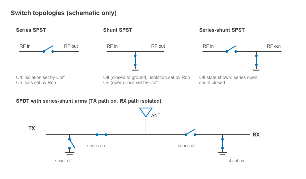
Each throw is built from one of three arrangements of the switching device:
- Series: the device sits in line with the signal. Its on resistance sets the loss and its off capacitance sets the isolation, which falls with frequency.
- Shunt: the device connects the line to ground. When it conducts it reflects the signal and provides isolation; when it is off its capacitance loads the line and adds a little loss.
- Series-shunt: a series element plus a shunt element on the output side. In the off state the series device blocks and the shunt device grounds whatever leaks through. This is the usual choice for high isolation.
A reflective switch presents a short or open to the unused port, which returns the signal toward its source. An absorptive (terminated) switch switches a 50 Ω load onto the off port so that it stays matched. Absorptive parts suit test systems and amplifier inputs, at the cost of slightly more loss and a lower power rating.
Key Specifications
Insertion loss
A series element of impedance Z between two Z0 ports has S21 = 2Z0 / (2Z0 + Z). A shunt admittance Y gives S21 = 2 / (2 + YZ0). For a conducting series device with on resistance Ron, the loss is IL = 20log(1 + Ron/2Z0) dB. In a receive path every tenth of a decibel of switch loss adds directly to the system noise figure, and in a transmit path it is lost output power, which is why antenna switches are usually specified to a few tenths of a decibel.
Isolation
Isolation is |S21| in the off state, expressed as a positive number of decibels. For a series device with off capacitance Coff, Z = 1/(jωCoff), and isolation falls by roughly 6 dB per octave once |Z| is comparable to 2Z0. Packaging, bond wires and board coupling eventually limit isolation regardless of the die.
Power handling and linearity
The off-state device must block the full RF voltage. In a matched 50 Ω system the peak voltage is Vpk = √(2PZ0), and a mismatched load can raise it by up to (1 + |Γ|). Datasheets quote compression points, IP3 and harmonics. Because switches feed antennas directly, harmonics generated in the switch are radiated, so the second and third harmonic at full transmit power are often the specifications that matter most. The intermodulation and intercept page explains how IP3 is defined.
Switching speed
Datasheets usually separate the rise and fall time of the RF envelope (10 % to 90 %) from the full switching time measured from the control edge (50 % control to 90 % RF). Fast control edges also couple into the RF path as video leakage, a baseband transient that can upset a following detector.
Worked Example: Series, Shunt and Series-Shunt FET Switches
Take a FET with Ron = 1.5 Ω and Coff = 150 fF in a 50 Ω system. These are example values chosen to illustrate the method, not the data of a specific part.
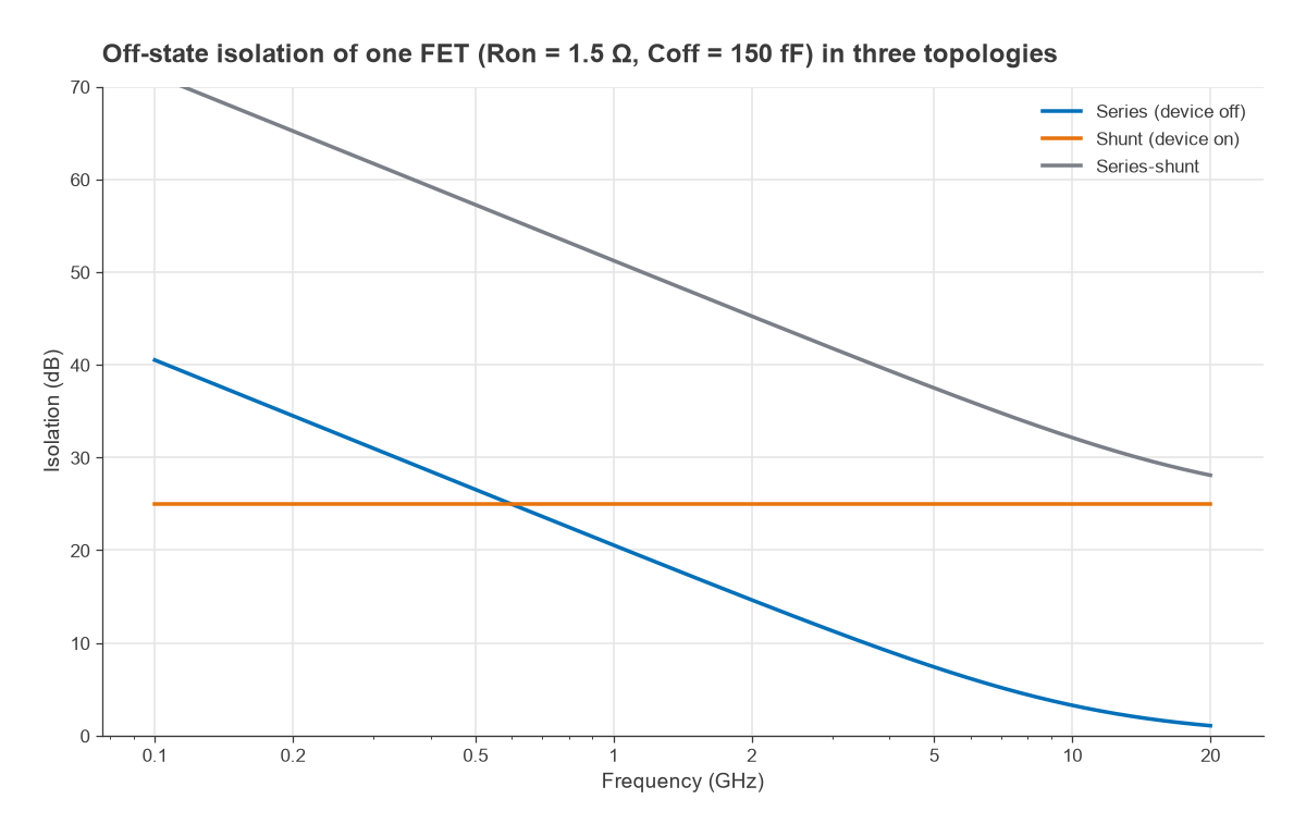
- Figure of merit: Ron·Coff = 225 fs, so the switch cutoff frequency fc = 1/(2πRonCoff) = 707 GHz.
- Series on-state loss: 20log(1 + 1.5/100) = 0.129 dB.
- Series off-state at 2 GHz: |Z| = 1/(2π × 2 × 109 × 150 × 10−15) = 530.5 Ω, so |S21| = 100/|100 − j530.5| = 0.185, which is 14.6 dB of isolation.
- Shunt device conducting: |S21| = 2/(2 + 50/1.5) = 0.0566, or 24.9 dB, independent of frequency in this simple model.
- Series-shunt combination at 2 GHz: cascading the two ABCD matrices gives 45.2 dB. That is about 6 dB more than the sum of the two individual values (39.5 dB), because the leakage through the series capacitance now meets a near-short instead of a 50 Ω load.
At 2.4 GHz the series-shunt on state (series device on, shunt device off) has 0.14 dB of loss and the off state 43.7 dB of isolation. The same FET used only in series gives just 13.1 dB, which is why single-element series switches are uncommon above a few hundred megahertz unless isolation is unimportant.
Device width and the Ron·Coff product
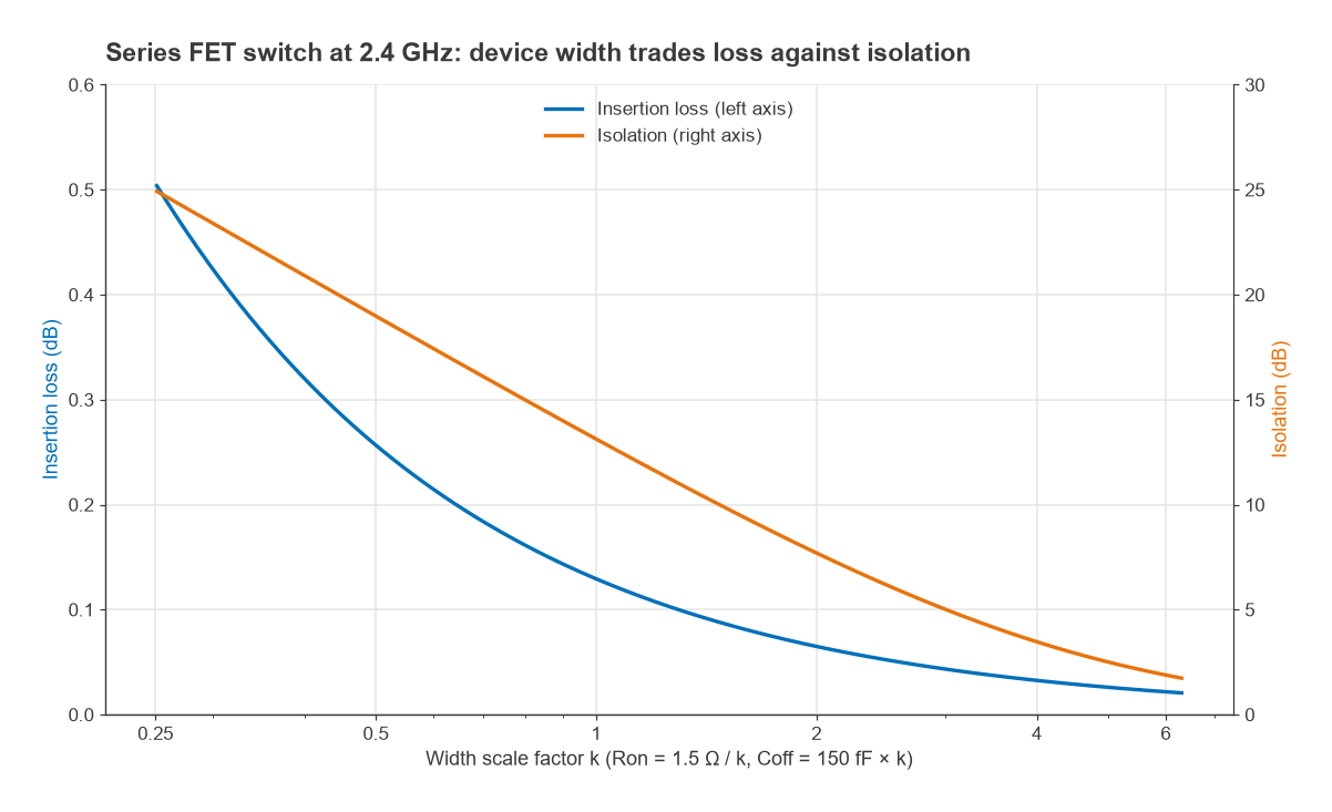
Making a FET k times wider divides Ron by k and multiplies Coff by k, so the product stays fixed. For the series switch at 2.4 GHz, k = 0.5 gives 0.26 dB loss and 19.0 dB isolation, k = 2 gives 0.065 dB and 7.7 dB, and k = 4 gives 0.033 dB and 3.5 dB. Width moves the operating point along a fixed trade-off curve, while only a better process (a lower Ron·Coff) moves the curve itself. That is why Ron·Coff is the standard way to compare switch processes.
PIN Diode Switches
A PIN diode has a wide intrinsic region between its p and n layers. Under forward bias the region floods with stored charge and behaves as a small resistance Rs, set by the bias current. Under reverse or zero bias it behaves as a small junction capacitance Cj. Because the stored charge cannot follow the RF cycle, the diode acts as a linear resistor rather than a rectifier as long as the signal frequency is well above 1/(2πτ), where τ is the carrier lifetime. For τ = 1 µs that corner is 159 kHz, so PIN switches work from a few megahertz upward.
With example values Rs = 1 Ω and Cj = 0.1 pF, a series PIN switch has 0.086 dB of loss and, at 2 GHz, 18.1 dB of isolation. A shunt PIN diode conducting at 1 Ω gives 28.3 dB. PIN switches handle high power and stay linear because the stored charge holds the diode in its state even during large voltage swings. The cost is the bias network: DC blocks, RF chokes and a driver supplying forward current and reverse voltage. Switching speed is limited by how fast that charge can be injected and removed, typically in the range of tens of nanoseconds to microseconds depending on the diode and the driver.
FET Switches: GaAs and SOI
A FET switch uses the channel as a voltage-controlled resistor, so the gate draws almost no current. GaAs pHEMT switches came first and still offer good Ron·Coff at microwave frequencies. Silicon-on-insulator CMOS has taken over most cellular and Wi-Fi antenna switching because it can integrate the switch, control logic, negative-voltage generator and digital interface on one die. The buried oxide isolates each transistor from the substrate, which keeps parasitic capacitance low and allows many devices to be stacked in series.
Stacking is how FET switches reach watt-level power. Consider 36 dBm (3.98 W) in 50 Ω. The peak voltage is √(2 × 3.98 × 50) = 20.0 V, and a 3:1 VSWR (|Γ| = 0.5) can raise it to 29.9 V. If each device in the stack is assumed, for illustration, to block about 2.5 V safely, about 12 devices are needed in each off arm. Stacking N devices multiplies Ron by N and divides Coff by N, so the Ron·Coff product survives, but the die grows. The transistor families behind these processes are compared in RF transistor technologies.
MEMS and Electromechanical Switches
A MEMS switch moves a microscopic metal beam or membrane to make or break contact (ohmic type) or to change a capacitance (capacitive type). Because the closed path is metal, loss is very low and the linearity is excellent, often far beyond any semiconductor switch. The drawbacks are mechanical. Switching takes microseconds rather than nanoseconds, actuation often needs tens of volts generated on chip, hot switching under RF power shortens contact life, and the parts need hermetic or near-hermetic packaging. Coaxial electromechanical relays go further still, with millisecond switching, and are common in test racks.
PIN vs FET vs MEMS Comparison
The table gives qualitative positions and approximate typical ranges as of 2026. Individual parts vary widely, so the datasheet always takes precedence.
| Property | PIN diode | GaAs / SOI FET | MEMS |
|---|---|---|---|
| Insertion loss | Low | Low to moderate, rises with throw count | Lowest |
| Isolation | High in series-shunt form | Moderate to high, falls with frequency | High |
| Power handling | Highest, up to high-power transmitters | Watt-level with stacking | Limited by hot switching |
| Linearity | High at high power | Good, limited by stack and substrate | Very high |
| Switching speed | Roughly tens of ns to µs, driver-dependent | Roughly tens of ns to a few µs | Microseconds or slower |
| Control power | Bias current needed | Near zero | Near zero, but high actuation voltage |
| Low-frequency limit | Set by carrier lifetime | Can operate down to very low frequencies | Down to DC for ohmic types |
| Integration | Discrete or hybrid | Highly integrated with logic | Specialised process and package |
Choosing an RF Switch
- Start with the worst-case RF voltage, including mismatch, rather than the nominal power.
- Decide whether the off port must stay matched; if so, choose an absorptive part.
- Check harmonics and IMD at the actual transmit power when the switch feeds an antenna. Multi-band systems with several simultaneous carriers are especially sensitive, as discussed in RF coexistence.
- Compare switching and settling time with the protocol’s guard time, and check video leakage if a detector or ADC follows.
- For a TX/RX changeover, compare the switch with alternatives such as a circulator or a duplexer.
Integrated switches usually share a package with filters and amplifiers, as described in RF front-end modules, and phased arrays use them in each element (see phased array design).
Frequently Asked Questions
PIN diode vs SOI switch: which should I use?
Use a PIN diode switch when power handling and linearity at high power come first and a bias supply is acceptable. Use an SOI switch for low to moderate power where low control current, small size, many throws and a digital interface matter more.
Why does switch isolation fall at high frequency?
The off-state device is essentially a capacitor, and its reactance drops as frequency rises, letting more signal through. Package and layout coupling add further paths. Series-shunt topologies and additional shunt sections recover some of the loss of isolation.
What does Ron·Coff mean?
It is the product of a switch device’s on resistance and off capacitance, usually quoted in femtoseconds. It is independent of device width, so it measures the process itself: a lower value means less loss for a given isolation.
Related Topics
Other components in the RF passive components hub include RF attenuators, directional couplers, hybrid couplers and the Wilkinson power divider. For definitions of the terms used here, see the wireless terms glossary.