

To design a pi attenuator, convert the attenuation A in dB to a voltage ratio K = 10A/20, then set each shunt resistor to Z0(K + 1)/(K − 1) and the series resistor to Z0(K2 − 1)/(2K). An RF attenuator is a resistive network that reduces signal power by a fixed amount while keeping the input and output matched to the system impedance, unlike a simple series resistor or divider.
Attenuators, often called pads, are among the simplest RF components and among the most useful. They set signal levels into mixers and ADCs, protect test equipment, improve the match seen by a sensitive stage, and isolate an oscillator from load changes. This page gives the design formulas for matched pi, T and bridged-T attenuators, a table of standard values, the power rating calculation that is easy to get wrong, and a calculator. It belongs to the RF passive components section of the RF design reference.
What a matched attenuator does
A matched attenuator has two properties at once. Its insertion loss equals the design attenuation when it sits between source and load impedances of Z0, and its input impedance is Z0 when its output is terminated in Z0, and the same in the other direction. A single series resistor reduces power but presents a mismatch; a matched pad does not. Because the network is purely resistive, the attenuation is in principle independent of frequency, and in practice it stays flat until component parasitics take over.
All of the design formulas use the voltage ratio
K = 10A/20
so that a 10 dB pad has K = 3.1623 and a 6 dB pad has K = 1.9953. Reflection quantities used below are defined in VSWR and return loss.
Pi, T and bridged-T formulas
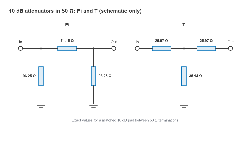
Pi attenuator
The pi pad has a shunt resistor at each port and a series resistor between them:
- Shunt resistors (each): Rshunt = Z0(K + 1)/(K − 1)
- Series resistor: Rseries = Z0(K2 − 1)/(2K)
T attenuator
The T pad has a series resistor at each port and a shunt resistor at the centre:
- Series resistors (each): Rseries = Z0(K − 1)/(K + 1)
- Shunt resistor: Rshunt = 2Z0K/(K2 − 1)
Bridged-T attenuator
The bridged-T uses two series resistors equal to Z0, a bridging resistor R1 across them and a shunt resistor R2 from their junction to ground:
- Bridge resistor: R1 = Z0(K − 1)
- Shunt resistor: R2 = Z0/(K − 1)
Since only R1 and R2 change with attenuation, and their product is always Z02, the bridged-T suits variable attenuators in which two elements are adjusted together.
Choosing between pi and T
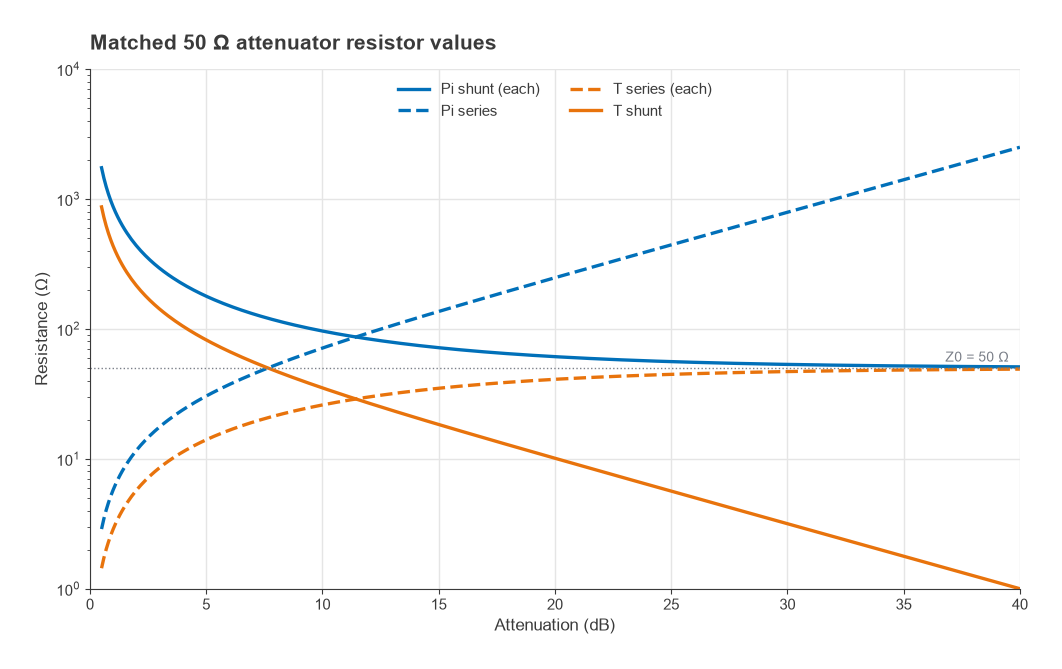
Pi and T pads of the same value are electrically equivalent at low frequencies. The choice is usually practical. At high attenuation the pi series resistor and the T shunt resistor become extreme: for 30 dB in 50 Ω, the pi series arm is 789.8 Ω and the T shunt arm is 3.17 Ω. Very small resistances are hard to realize accurately because pad and via resistance add to them, and very large ones are bypassed by their own parasitic capacitance at high frequency. Pi pads are common in printed layouts because both shunt resistors can be placed right at the ground vias, while T pads place the low-value shunt resistor at a single point.
Worked example: a 10 dB pad in 50 Ω
- K = 1010/20 = 3.1623.
- Pi shunt: 50 × 4.1623/2.1623 = 96.25 Ω. Pi series: 50 × (10 − 1)/(2 × 3.1623) = 71.15 Ω.
- T series: 50 × 2.1623/4.1623 = 25.97 Ω. T shunt: 2 × 50 × 3.1623/9 = 35.14 Ω.
- Round to the nearest E96 values. For the pi pad, 95.3 Ω and 71.5 Ω give 10.07 dB of attenuation and 53.8 dB return loss. For the T pad, 26.1 Ω and 34.8 Ω give 10.07 dB and 73.9 dB return loss.
The rounding error is negligible compared with resistor tolerance and parasitic effects, so 1 % resistors from a standard series are adequate for most fixed pads.
Standard attenuator values (50 Ω)
| Attenuation (dB) | Pi shunt (Ω) | Pi series (Ω) | T series (Ω) | T shunt (Ω) | Bridged-T R1 (Ω) | Bridged-T R2 (Ω) |
|---|---|---|---|---|---|---|
| 1 | 869.55 | 5.77 | 2.88 | 433.34 | 6.10 | 409.77 |
| 3 | 292.40 | 17.61 | 8.55 | 141.93 | 20.63 | 121.20 |
| 6 | 150.48 | 37.35 | 16.61 | 66.93 | 49.76 | 50.24 |
| 10 | 96.25 | 71.15 | 25.97 | 35.14 | 108.11 | 23.12 |
| 20 | 61.11 | 247.50 | 40.91 | 10.10 | 450.00 | 5.56 |
| 30 | 53.27 | 789.78 | 46.93 | 3.17 | 1531.14 | 1.63 |
As attenuation rises, the pi shunt and T series resistors approach Z0, while the pi series resistor grows without limit and the T shunt resistor falls toward zero. Values for 75 Ω systems scale directly by 75/50.
Power rating
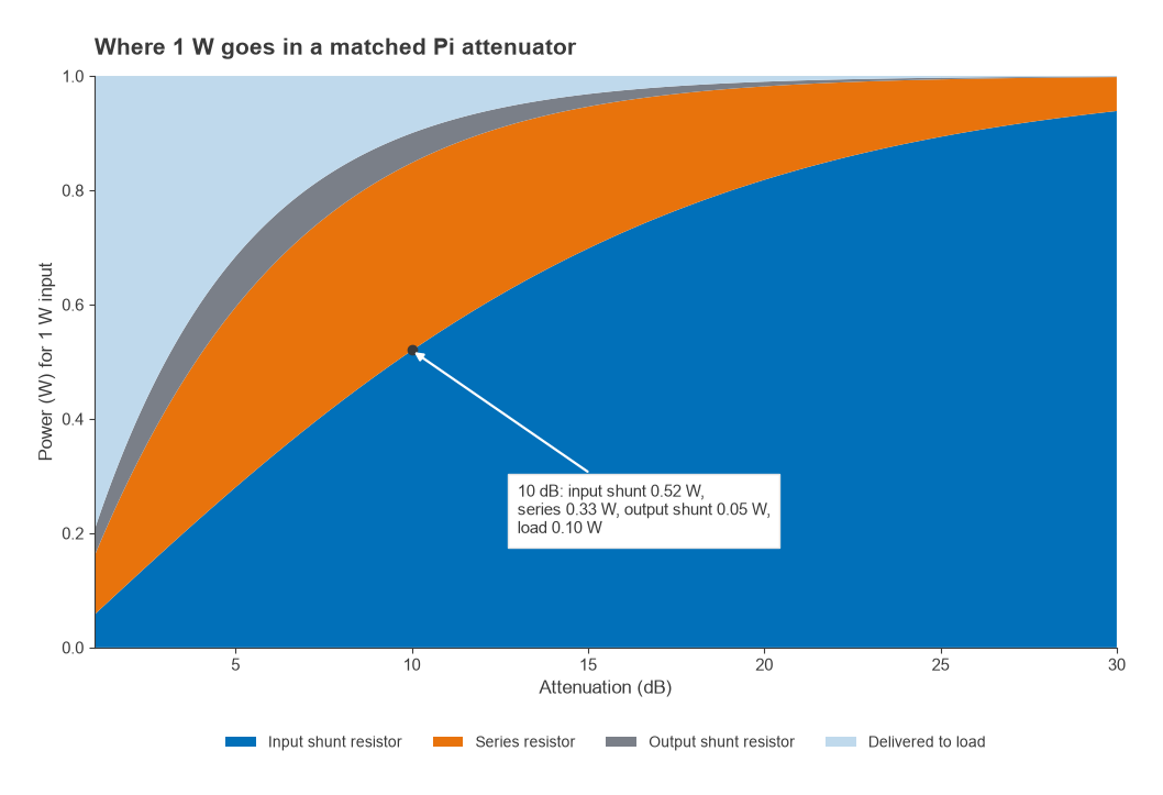
The resistor nearest the source dissipates most of the power, and it is easy to undersize. For a matched pi pad with input power Pin, the input voltage is V1 = √(PinZ0) and the output voltage is V2 = V1/K. The dissipations are
- Input shunt: V12/Rshunt
- Series: (V1 − V2)2/Rseries
- Output shunt: V22/Rshunt
For 1 W into the 10 dB pad, V1 = 7.07 V and V2 = 2.24 V. The input shunt resistor dissipates 0.52 W, the series resistor 0.33 W and the output shunt 0.05 W, and 0.10 W reaches the load. The total is 1.00 W, as it must be. A matched T pad of the same value happens to split power in the same proportions, with the input series resistor taking 0.52 W. At 20 dB the input resistor of a pi pad takes 0.82 W of every watt applied. In a bridged-T pad the hottest part is the fixed Z0 arm on the input side, which takes 0.47 W of 1 W at 10 dB. A pad intended to handle 1 W therefore needs an input resistor rated well above 0.5 W, not a set of resistors each rated for a third of the total.
Resistor ratings also fall with temperature, and data sheets typically give a derating curve above a stated case or terminal temperature. Splitting the hot resistor into several parallel or series parts spreads the heat. If the pad may see full power from the output side, for example when a transmitter is connected the wrong way round, both ends must be rated for it. Thermal design for higher powers is discussed in RF PA thermal design.
Improving match with a pad
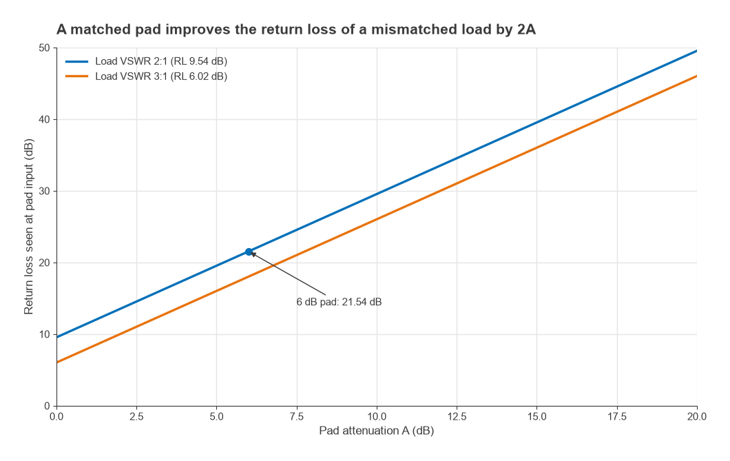
A reflection from a poorly matched load passes through the pad twice, so a matched pad of A dB improves the return loss seen at its input by 2A dB, assuming the pad’s own match is much better. A load with VSWR 2:1 has a return loss of 9.54 dB. Behind a 6 dB pad it appears as 21.54 dB, equivalent to a VSWR of about 1.18:1. This is why a few decibels of attenuation are often placed in front of a mixer, a filter whose out-of-band impedance is reactive, or a test port. The same effect reduces mismatch uncertainty in power measurements. The price is the attenuation itself, which adds directly to noise figure when the pad sits ahead of a receiver, as explained in noise figure.
Step attenuators and frequency limits
A step attenuator cascades switched sections, usually with binary weights such as 0.5, 1, 2, 4, 8 and 16 dB, giving 0 to 31.5 dB in 0.5 dB steps with six control bits. Each section is a pi or T pad that is either switched in or bypassed. Mechanical step attenuators are used in test equipment, while integrated digital step attenuators use transistor switches and are common in receiver gain control and transmitter level setting. Their specifications to check are the insertion loss in the 0 dB state, step accuracy, phase change between states, switching time and the transient that can occur while several bits change at once. The switch technology behind them is covered in RF switches.
Fixed pads made from surface-mount resistors work well into the low gigahertz range. Above that, the inductance of each resistor and its pads, and the capacitance across large-value resistors, start to change the attenuation and the match. Thin-film attenuator chips, in which the whole network is printed on one substrate, extend the usable range much further. For a discrete layout, smaller packages, short connections and ground vias placed directly at each shunt resistor help, as discussed in RF component parasitics and RF grounding and via stitching.
Pads between unequal impedances
An attenuator can also match two different impedances. The two-resistor minimum-loss pad from Z1 to a lower Z2 uses a series resistor √(Z1(Z1 − Z2)) on the Z1 side and a shunt resistor Z2√(Z1/(Z1 − Z2)) on the Z2 side. For 75 Ω to 50 Ω these are 43.30 Ω and 86.60 Ω, and the loss is 20log(√1.5 + √0.5) = 5.72 dB. Lossless alternatives are covered in impedance matching.
Pi and T attenuator calculator
Enter the attenuation, system impedance and input power. The calculator returns exact resistor values, the nearest E96 values, the attenuation and return loss obtained with those E96 values, and the power dissipated in each resistor of the exact design.
The bridged-T fixed arms are assumed to be exactly Z0; with E96 parts the nearest value (49.9 Ω for a 50 Ω system) would be used in practice.
Frequently asked questions
How do you design a pi attenuator?
Calculate K = 10A/20 from the required attenuation. Each shunt resistor is Z0(K + 1)/(K − 1) and the series resistor is Z0(K2 − 1)/(2K). Round to standard values, check the input resistor’s power rating, and keep shunt resistors close to their ground vias.
What is the difference between a pi and a T attenuator?
Both give the same attenuation and match. A pi pad has two shunt resistors and one series resistor; a T pad has two series resistors and one shunt resistor. The choice depends on which gives more practical resistor values and a cleaner layout at the frequency of interest.
Which resistor in an attenuator gets hottest?
The resistor at the input. In a 10 dB pi pad the input shunt resistor dissipates about 52 % of the input power, and in a 20 dB pad about 82 %. It must be rated for that share, with derating for temperature.
Why put an attenuator in front of a mixer or test port?
A matched pad improves the return loss seen at its input by twice its attenuation, so a poorly matched port looks much closer to Z0. That stabilizes the behaviour of the preceding stage and reduces mismatch errors, at the cost of signal level and noise figure.
Related topics
Other passive building blocks in this section include directional couplers, the Wilkinson power divider and hybrid couplers. Decibel conversions are explained in dB, dBm and dBc, other calculators are collected on the RF calculators page, and short definitions are in the wireless terms glossary.