

PA thermal management is the part of RF power amplifier design that keeps the transistor junction below its rated temperature by moving dissipated power through a chain of thermal resistances into the air. Silicon LDMOS and GaN-on-SiC devices are typically rated for a maximum junction temperature of about 200 to 225 °C, GaAs parts lower, but long life usually needs a design junction temperature well below that limit, often 150 to 175 °C or less.
The method is the same for a 2 W driver and a 500 W pallet: find the heat, add up the thermal resistances and check the junction temperature against the reliability target. This page belongs to the RF amplifiers section of the RF design guide and follows on from power amplifier classes, since the class and efficiency of the stage decide how much heat there is to remove.
How Much Heat a PA Produces
Energy is conserved, so everything that enters the transistor and does not leave as RF output becomes heat. The dissipated power is
Pdiss = PDC + Pin − Pout
where PDC = VDD · ID is the supply power. With drain efficiency η = Pout/PDC, this becomes Pdiss = Pout(1/η − 1) + Pin. Dissipation rises steeply as efficiency falls: a 50 W amplifier at 70 % efficiency dissipates about 23 W, while the same output at 40 % dissipates about 77 W. The worst case is not always full power either. A class AB stage carrying a high peak-to-average signal spends most of its time backed off at low efficiency, and a mismatched load can raise dissipation further. Design for the worst operating point the product will meet.
Efficiency figures come from the load-pull data or the datasheet at the actual load and bias; the RF amplifier datasheet guide explains which efficiency definition each table uses. Drain efficiency ignores the input drive, while power-added efficiency (PAE) subtracts it, so dissipation computed from PAE needs the input power added back in the same way as above.
The Thermal Resistance Chain
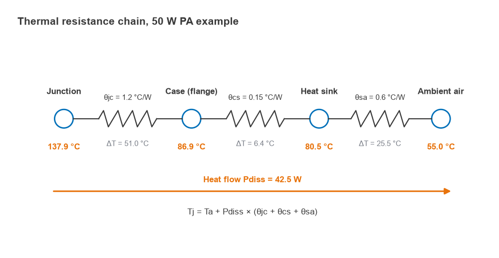
Heat flows from the junction (the hot channel region under the gate) through the die, the die attach and the package flange, across the interface material, into the heat sink and finally into the air or coolant. Each step has a thermal resistance θ in °C/W, defined as the temperature difference across it divided by the heat flowing through it. In steady state the steps are in series, exactly like resistors carrying the same current, so
Tj = Ta + Pdiss · (θjc + θcs + θsa)
- θjc, junction to case. Fixed by the device and package. It depends on die material, thickness, die attach and flange, and is quoted at a stated case reference point.
- θcs, case to sink. The interface: solder, indium foil, thermal grease, a graphite pad or a printed circuit board with thermal vias. It depends on contact area, flatness, mounting pressure and material, and it is the term most often underestimated.
- θsa, sink to ambient. The heat sink and its airflow, or a cold plate and its coolant flow. Fin geometry, air speed and the temperature rise of the air as it crosses the fins all matter.
When the transistor sits on a board rather than directly on a heat sink, θcs becomes the resistance of the copper and via array under the package. Its resistance falls roughly in proportion to the number of vias; filled vias, a copper coin or a cut-out that lets the flange bolt to the sink bring it down further. The same via arrays also form the RF ground under the device, which is covered in RF grounding and via stitching.
Junction Temperature Calculation, Step by Step
- Find the worst-case operating point: output power, efficiency and input drive at the highest supply voltage, the worst load VSWR the design must survive, and the highest ambient temperature.
- Compute Pdiss = PDC + Pin − Pout.
- Take θjc from the datasheet at a case temperature close to the expected one, since it increases with temperature for most semiconductors.
- Estimate θcs from the interface material data and contact area, and θsa from the heat-sink data at the actual airflow.
- Add the temperature rises from ambient upward and compare Tj with the design limit, not the absolute maximum rating.
- If Tj is too high, work backward to the maximum allowed θsa and choose the cooling to meet it with margin.
Worked example: 50 W GaN stage
A GaN amplifier delivers Pout = 50 W with 15 dB gain and 55 % drain efficiency. The device has θjc = 1.2 °C/W, the flange is mounted with a thin thermal pad giving θcs = 0.15 °C/W, and a forced-air heat sink provides θsa = 0.6 °C/W. The maximum ambient inside the enclosure is 55 °C.
- PDC = 50 / 0.55 = 90.9 W
- Pin = 50 / 101.5 = 1.58 W
- Pdiss = 90.9 + 1.58 − 50 = 42.5 W
- Heat sink: Ts = 55 + 42.5 × 0.6 = 80.5 °C
- Case: Tc = 80.5 + 42.5 × 0.15 = 86.9 °C
- Junction: Tj = 86.9 + 42.5 × 1.2 = 137.9 °C
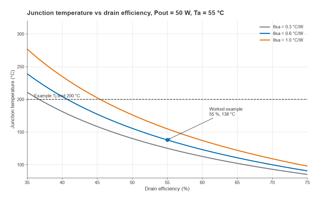
The junction runs at about 138 °C. More than half of the 83 °C total rise is inside the package, which is typical of modern high-power-density devices and is why the interface and heat sink cannot make up for a poor device choice. Working backward, a 200 °C limit would allow θsa up to (200 − 55)/42.5 − 1.35 = 2.06 °C/W, and a 175 °C limit would allow 1.47 °C/W. If the thermal pad were replaced by a poorly applied interface with θcs = 0.5 °C/W, the junction would rise to 152.7 °C, an increase of 15 °C from the interface alone.
Figure 2 shows the same calculation across a range of efficiencies. Below about 41 % drain efficiency, the 0.6 °C/W sink would no longer hold the junction under 200 °C at full output. This is the thermal reason that efficiency enhancement and PA linearization, which allows a stage to run closer to compression, matter as much as they do.
How Hot Can an RF Transistor Get?
Every device has an absolute maximum junction temperature, and the approximate values vary with the technology described in RF transistor technologies. GaN-on-SiC HEMTs are commonly rated around 225 °C, silicon LDMOS around 200 to 225 °C, GaAs pHEMT and HBT parts around 150 to 175 °C, and silicon and SiGe ICs around 125 to 150 °C. These are typical ranges, and the datasheet of the actual part governs.
The absolute maximum is a survival limit, not an operating point. Running at it shortens life sharply, as the next section shows, and leaves no margin for the hot spots that a uniform θjc hides. Peak channel temperature in a multi-finger device is also higher than the average junction temperature that simple models report.
MTTF vs Junction Temperature
Most semiconductor wear-out mechanisms, such as gate metal diffusion, electromigration and trap generation, are thermally activated. Their rate follows the Arrhenius relation, so the mean time to failure scales as
MTTF(T1) / MTTF(T2) = exp[(Ea/k) · (1/T1 − 1/T2)]
with temperatures in kelvin, Boltzmann’s constant k = 8.617 × 10⁻⁵ eV/K and Ea the activation energy of the dominant mechanism. Manufacturers extract Ea and the absolute MTTF from accelerated life tests at several high temperatures. Values between roughly 0.7 and 2 eV are commonly reported for RF transistor technologies, so the curves in Figure 3 use 0.7, 1.0 and 1.5 eV as illustrations rather than data for any particular device.
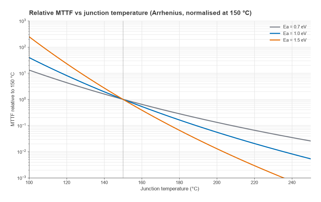
The effect is large. With Ea = 1.0 eV, reducing the junction from 148 °C to 138 °C, a 10 °C change, increases MTTF by a factor of 1.96. Running at 150 °C instead of 200 °C gives a factor of 18. With Ea = 1.5 eV the same 50 °C reduction gives a factor of 77. The common rule that every 10 °C halves life is the Ea ≈ 1 eV case near 150 °C, and it understates the benefit for higher activation energies.
Datasheet MTTF curves describe the intrinsic semiconductor. Solder fatigue from temperature cycling and failed fans also limit field life, and a cooler, steadier junction helps with both.
Pulsed Operation and Transient Thermal Impedance
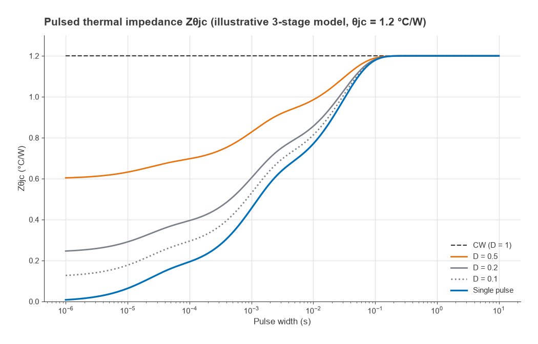
A radar or burst transmitter dissipates heat in short pulses. The die and package have thermal capacitance as well as resistance, so a short pulse does not heat the junction as much as a continuous signal at the same peak dissipation. Datasheets capture this with a transient thermal impedance Zθjc(tp, D), plotted against pulse width tp for several duty cycles D. It is often modelled as a Foster network of resistor and capacitor pairs:
Zsingle(t) = Σ Ri (1 − e−t/τi), Z(tp, D) ≈ D · θjc + (1 − D) · Zsingle(tp)
The second expression is a common approximation for a long train of equal pulses. Using the illustrative three-stage model in Figure 4 (R = 0.15, 0.45 and 0.6 °C/W with time constants of 20 µs, 1 ms and 30 ms), a 100 µs pulse at 10 % duty cycle gives Z ≈ 0.29 °C/W. A peak dissipation of 120 W then raises the junction 35.3 °C above the case, compared with 144 °C if the same 120 W were continuous. Pulses longer than about 100 ms behave as CW in this model, because the slowest time constant has settled. Using average power with the steady-state θjc would predict only 14.4 °C and would underestimate the peak junction temperature.
Choosing and Verifying the Cooling
Once the allowed θsa is known, the cooling method follows. Natural convection suits a few tens of watts at most; forced air typically reaches well under 1 °C/W for a moderate sink. Liquid cold plates and heat pipes serve kilowatt pallets and dense arrays such as the phased-array front ends in Part 18 of Radio Architectures, where the element spacing leaves little room for fins.
- Spread the heat before it reaches the interface. A thick copper or aluminium heat spreader under the flange lowers the effective θcs by enlarging the area that conducts into the sink.
- Keep interface layers thin and flat. Mounting screw torque and surface finish set the real θcs more than the datasheet value of the material.
- Measure. A thermocouple at the flange reference point confirms Tc, and Tj follows from Tc + Pdiss · θjc.
Temperature also shifts RF behaviour: gain usually falls and quiescent current changes as the device heats, which is why bias circuits often include temperature compensation, described in RF amplifier biasing.
Frequently Asked Questions
How hot can an RF transistor get?
The absolute maximum junction temperature is typically about 200 to 225 °C for GaN-on-SiC and LDMOS devices and lower for GaAs and silicon ICs. For long life, designs usually target a junction temperature well below that, often 150 to 175 °C or less, as set by the manufacturer’s MTTF data.
How do I size a heat sink for an RF amplifier?
Compute the worst-case dissipation, then solve θsa = (Tj,max − Ta)/Pdiss − θjc − θcs. Choose a sink and airflow with a thermal resistance comfortably below that value at the real air speed.
Can I use average power for a pulsed amplifier?
No. Average power with the steady-state θjc underestimates the peak junction temperature. Use the transient thermal impedance at the actual pulse width and duty cycle with the peak dissipation.
Related Topics
The RF amplifiers hub links every amplifier topic on the site. Efficiency and class selection are covered in power amplifier classes, and the trade between low-noise, gain-block and power stages in LNA vs gain block vs PA. For the small-signal end of the chain, see design of low-noise amplifiers, and for terms used here, the wireless terms glossary.