

Phase noise is the random fluctuation in the phase of an oscillator’s output, which spreads a spectral line that should be a single frequency into a carrier with noise sidebands. It is specified as L(f), the single-sideband noise power in a 1 Hz bandwidth at an offset f from the carrier, relative to the carrier power, in dBc/Hz. In an RF system it sets the jitter of clocks, the EVM floor of transmitters and receivers, and how well a receiver tolerates strong nearby signals.
Phase noise belongs to the RF noise branch of the RF design map. It is the oscillator’s counterpart to the additive noise described by thermal noise (kTB) and noise figure: instead of adding to the signal, it modulates the signal’s phase.
Definition: L(f) in dBc/Hz
An ideal oscillator produces v(t) = A cos(2πf0t). A real one produces v(t) = A(t) cos(2πf0t + φ(t)), where φ(t) is a random phase process and A(t) carries a much smaller amplitude noise. Most oscillators limit their amplitude, so the phase term dominates close to the carrier. The modern definition, standardized by the IEEE, is
L(f) = Sφ(f) / 2
where Sφ(f) is the one-sided power spectral density of the phase fluctuations in rad2/Hz. For small phase deviations this equals the more intuitive measurement definition:
L(f) = 10log(PSSB(f0 + f, 1 Hz) / Pcarrier) dBc/Hz
The units deserve a careful reading. “dBc” means decibels relative to the carrier. “/Hz” means the noise is normalized to a 1 Hz bandwidth, so a value of −120 dBc/Hz at 1 MHz offset means that a 1 Hz slice of noise, 1 MHz away from the carrier, is 120 dB weaker than the carrier itself. To find the noise in a real bandwidth B, add 10log(B): over a 200 kHz channel the same density amounts to −120 + 53.0 = −67 dBc of total noise, assuming the density is roughly flat across the channel.
Two quick rules help in practice. Multiplying an oscillator’s frequency by N raises its phase noise by 20log(N) at the same offset, which is why a 10 MHz reference multiplied to 2.4 GHz (N = 240) appears 47.6 dB noisier at the output of an ideal multiplier or in the passband of a PLL. Dividing by N lowers it by the same amount until the divider’s own noise floor is reached.
Leeson’s Model of Oscillator Phase Noise
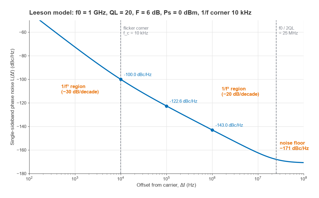
D. B. Leeson’s 1966 model explains the shape of a typical oscillator phase noise curve with a feedback argument. The active device adds white noise with density FkT, where F is its effective noise factor. The resonator, with loaded quality factor QL, has a half-bandwidth of f0/(2QL). Inside that half-bandwidth the loop integrates phase perturbations, turning white phase noise into noise that falls at 20 dB per decade. Flicker noise in the device adds a further 10 dB per decade below the corner frequency fc. The result is
L(Δf) = 10log[ (FkT / 2Ps) × (1 + (f0 / 2QLΔf)2) × (1 + fc/Δf) ]
where Ps is the signal power at the resonator, k is Boltzmann’s constant and T is the temperature. The model is semi-empirical. F is usually found by fitting measured data rather than from the device’s small-signal noise figure, and fc in an oscillator is not always the device’s flicker corner. Its value lies in the design guidance it gives: phase noise improves by 20 dB per decade of resonator Q, by 10 dB per decade of signal power, and by keeping the flicker corner low.
Worked example: a 1 GHz oscillator
Take f0 = 1 GHz, QL = 20, F = 6 dB, Ps = 0 dBm and fc = 10 kHz. With kT = −174 dBm/Hz at room temperature:
- Floor: 10log(FkT/2Ps) = −174 + 6 − 3 − 0 = −171 dBc/Hz.
- Resonator half-bandwidth: f0/(2QL) = 25 MHz.
- At Δf = 100 kHz: (25 MHz / 100 kHz)2 = 62,500, or +48.0 dB; flicker term 1.1, or +0.4 dB. L = −171 + 48.0 + 0.4 = −122.6 dBc/Hz.
- At 1 MHz: L = −143.0 dBc/Hz. At 10 kHz: L = −100.0 dBc/Hz.
Doubling QL to 40 would improve every point in the 1/f2 region by 6 dB. That is the reason high-Q resonators, from crystals to dielectric resonators, set the best achievable phase noise, as discussed in TCXO vs OCXO and VCO design. The Q-factor page covers how loaded Q is defined and measured.
From Integrated Phase Noise to RMS Jitter and EVM
A single L(f) value describes noise at one offset. Many system requirements depend on the total phase error, which is found by integrating the phase noise over the offsets that matter. The integrated single-sideband noise is
A = ∫ 10L(f)/10 df, from f1 to f2
Both sidebands contribute to phase error, so the RMS phase error in radians is σφ = √(2A). Dividing by the angular carrier frequency gives the RMS time jitter:
tj,rms = σφ / (2πf0)
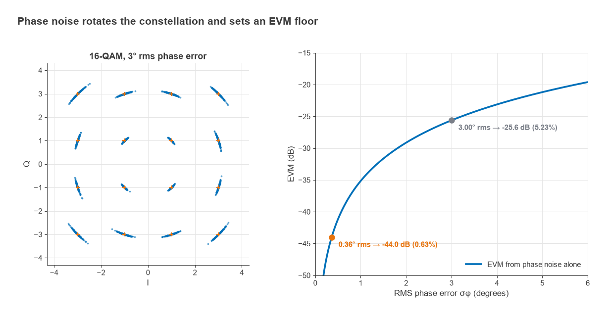
For a digitally modulated signal, a random phase error of σφ radians produces an error vector of rms magnitude √(2(1 − e−σφ²/2)), which is very close to σφ for small errors. A useful shortcut is EVM(%) ≈ 100 × σφ (rad). The limits f1 and f2 depend on the application. For an OFDM receiver, offsets much below the subcarrier spacing are largely tracked out as common phase error, while offsets above the channel bandwidth fall outside the signal.
Worked example: a 2.4 GHz synthesizer
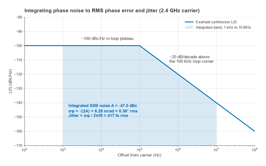
Model a synthesizer output as a flat −100 dBc/Hz from 1 kHz to the 100 kHz loop corner, then falling at 20 dB per decade to −140 dBc/Hz at 10 MHz. Integrate from 1 kHz to 10 MHz:
- Plateau: 10−10 × (100 kHz − 1 kHz) = 9.9 × 10⁻⁶.
- Slope: 10−10 × (105)2 × (1/105 − 1/107) = 9.9 × 10⁻⁶.
- A = 1.98 × 10⁻⁵, or −47.0 dBc.
- σφ = √(2 × 1.98 × 10−5) = 6.29 mrad = 0.36° rms.
- tj = 6.29 × 10⁻³ / (2π × 2.4 × 109) = 417 fs rms.
- EVM floor from phase noise alone: 0.63%, or −44.0 dB.
That floor is comfortable for most modulation formats. A noisier synthesizer with 3° rms phase error would give 5.2% EVM, or −25.6 dB, which would consume most of the error budget of a dense QAM signal before any other impairment is counted. The same jitter applied to a data converter clock limits SNR to −20log(2πfintj); 417 fs at a 1 GHz input gives about 51.6 dB, which is why sampling clocks for ADCs and direct RF sampling receive so much attention. Constellation effects are shown in more detail on the constellation diagrams page.
Reciprocal Mixing and Blocking
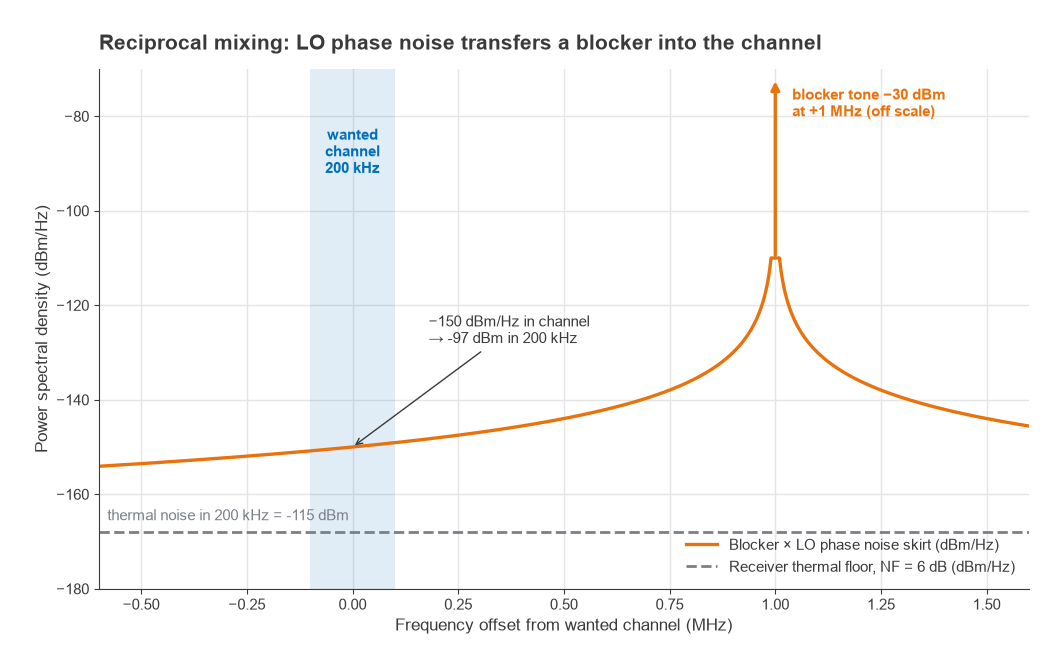
In a receiver the LO’s phase noise sidebands mix with every signal present at the mixer input, not only the wanted one. A strong unwanted signal at offset Δf from the wanted channel is translated by the LO’s noise skirt so that part of the skirt lands directly in the IF channel. This is reciprocal mixing, and it degrades sensitivity in the presence of a blocker even when the front end is perfectly linear. The noise it adds in the channel is approximately
NRM (dBm) = Pblocker (dBm) + L(Δf) (dBc/Hz) + 10log(B)
Take a −30 dBm blocker at 1 MHz offset, an LO with L(1 MHz) = −120 dBc/Hz and a 200 kHz channel. NRM = −30 − 120 + 53.0 = −97 dBm. The receiver’s own thermal noise in the same bandwidth with a 6 dB noise figure is −174 + 53.0 + 6 = −115 dBm. Reciprocal mixing dominates by 18 dB, and the receiver loses about 18 dB of sensitivity while the blocker is present. To push reciprocal mixing 10 dB below the thermal floor, the LO would need L(1 MHz) = −125 + 30 − 53 = −148 dBc/Hz. Requirements of this kind usually set the phase noise specification of a receiver’s synthesizer. Receiver blocking and desensitization covers how this combines with compression and intermodulation, and transmitters suffer the mirror-image problem when their phase noise falls into a neighbouring receive channel.
Reading Phase Noise Specifications
Datasheets usually give L(f) at a handful of decade offsets, for example 1 kHz, 10 kHz, 100 kHz and 1 MHz, together with integrated RMS jitter over a stated bandwidth. When comparing parts, check three things: the carrier frequency the numbers apply to (scale by 20log(N) to compare at a common frequency), the integration limits for jitter, and whether spurs are included in or excluded from the integration. A jitter figure integrated from 12 kHz to 20 MHz cannot be compared directly with one integrated from 1 kHz to 100 MHz. Measurement methods, including the spectrum analyzer approach and its limits, are covered in phase noise measurement.
Frequently asked questions
What is phase noise?
Phase noise is the random variation in an oscillator’s phase, seen in the spectrum as noise sidebands around the carrier. It is quantified by L(f), the single-sideband noise in 1 Hz at offset f relative to the carrier.
What does dBc/Hz mean?
It is noise power in a 1 Hz bandwidth expressed in decibels relative to the carrier power. To get the noise in a wider bandwidth B, add 10log(B), provided the density is roughly constant over that bandwidth.
How does phase noise affect EVM and reciprocal mixing?
Integrated phase noise gives an RMS phase error σφ, and EVM is approximately σφ in radians. In a receiver, the LO’s noise skirt transfers strong off-channel signals into the wanted channel, adding noise equal to the blocker power plus L(Δf) plus 10log of the channel bandwidth.
Phase noise vs jitter?
They describe the same impairment in different domains. Phase noise is the frequency-domain view, L(f) versus offset. Jitter is the time-domain view, the RMS timing error, found by integrating phase noise over a bandwidth and dividing the RMS phase error by 2πf0.
Related topics
The RF noise hub connects phase noise to the other noise topics. For how synthesizers shape phase noise, read frequency synthesis, PLLs and phase noise; for the oscillator itself, VCO design; and for the measurement, phase noise measurement. Definitions of related terms are collected in the wireless terms glossary.