

PLL loop filter design is the process of choosing the resistor and capacitor values between the charge pump and the VCO so that the phase-locked loop has a chosen bandwidth and phase margin. To design one, set the loop bandwidth from the phase noise and lock-time targets, pick a phase margin of about 45° to 60°, compute the filter’s zero and pole time constants, and then solve for the components from the charge pump current, VCO gain and divide ratio.
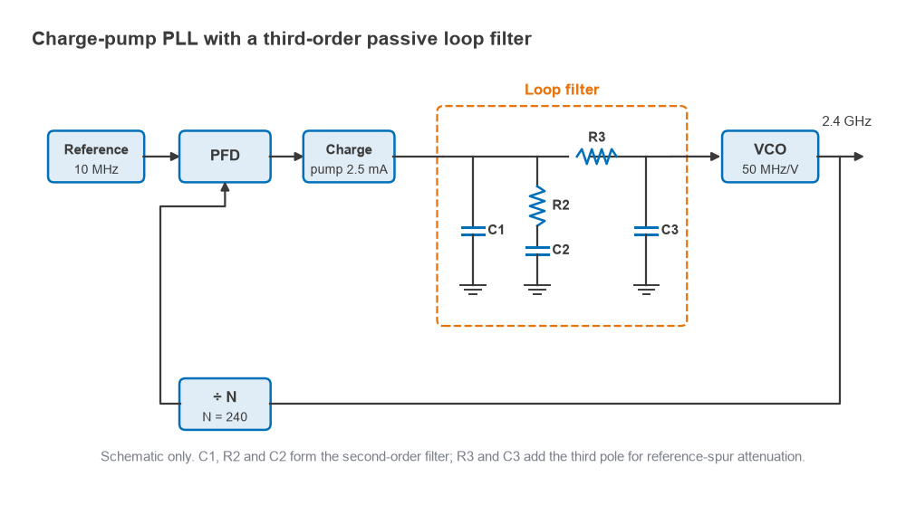
The loop filter sets how fast the loop locks, how much reference spur leaks through and where the output phase noise changes from PLL-dominated to VCO-dominated. This page covers the passive second- and third-order filters used with charge-pump PLLs, with a worked 2.4 GHz design. The architecture is introduced in PLLs, frequency synthesis and phase noise, part of the oscillators and frequency synthesis section of the RF design guide.
The Loop and Its Open-Loop Gain
In a charge-pump PLL the phase-frequency detector (PFD) compares the reference with the divided VCO output and switches a charge pump of current ICP. The phase detector gain is Kφ = ICP/2π in amperes per radian. The loop filter converts that current into a tuning voltage through its transimpedance Z(s), and the VCO converts voltage into frequency with gain KVCO, or Kv = 2πKVCO in rad/s per volt. Because the VCO integrates frequency into phase, the open-loop gain is
G(s) = Kφ Kv Z(s) / (N s)
where N is the feedback divide ratio. The loop bandwidth is usually defined as the frequency fc where |G| = 1, and the phase margin is 180° plus the phase of G at that frequency. The closed-loop transfer from the reference to the output is N·G/(1 + G), and from VCO noise to the output it is 1/(1 + G). That pair of transfer functions is why the bandwidth decides the phase noise profile.
Second-Order Passive Loop Filter Equations
The basic passive filter is a shunt capacitor C1 in parallel with a series branch R2–C2. Its transimpedance is
Z(s) = (1 + sT2) / [ s(C1 + C2)(1 + sT1) ], with T2 = R2C2 and T1 = R2C1C2/(C1 + C2)
The integrator 1/s gives the loop a second integration (a type 2 loop), so it settles with zero static phase error. The zero at 1/T2 provides phase lead for stability, and the pole at 1/T1 smooths the charge pump pulses. Maximum phase margin occurs at the geometric mean of the zero and pole, so the design places fc there:
- T1 = (sec φ − tan φ)/ωc, where φ is the target phase margin
- T2 = 1/(ωc2T1)
- C1 + C2 = (KφKv/(Nωc2)) × √[(1 + ωc2T22)/(1 + ωc2T12)]
- C1 = (C1 + C2)T1/T2, C2 = (C1 + C2) − C1, R2 = T2/C2
The third equation is simply |G(jωc)| = 1 solved for the total capacitance.
Third-Order Passive Loop Filter Equations
A second-order filter passes a significant fraction of the charge pump ripple at the PFD frequency, which modulates the VCO and produces reference spurs at fout ± fPFD. Adding a series R3 and shunt C3 in front of the VCO creates a third pole at 1/T3 that attenuates those spurs further. The transimpedance becomes
Z(s) = (1 + sT2) / [ s(A2s2 + A1s + A0) ]
with A0 = C1 + C2 + C3, A1 = C2R2(C1 + C3) + C3R3(C1 + C2) and A2 = C1C2C3R2R3. The denominator factors as A0(1 + sT1)(1 + sT3), so A1 = A0(T1 + T3) and A2 = A0T1T3. A widely used procedure, set out in Banerjee’s PLL design text, runs as follows:
- Choose the pole ratio T3/T1, commonly around 0.25. Larger values give more spur attenuation and less phase margin to work with.
- Solve numerically for T1 so that the phase margin tan−1(ωcT2) − tan−1(ωcT1) − tan−1(ωcT3) equals the target, with T2 = 1/(ωc2(T1 + T3)).
- Set A0 = (KφKv/(Nωc2)) × √[(1 + ωc2T22)/((1 + ωc2T12)(1 + ωc2T32))], then A1 and A2 from the time constants.
- Solve for the components: C1 = (A2/T22)[1 + √(1 + (T2/A2)(T2A0 − A1))], C3 = (−T22C12 + T2A1C1 − A2A0)/(T22C1 − A2), C2 = A0 − C1 − C3, R2 = T2/C2 and R3 = A2/(C1C3T2).
- Round to standard values and recheck fc and phase margin by evaluating G(jω) from the actual components.
Worked Example: 2.4 GHz Synthesizer
Design a filter for a 2.4 GHz output from a 10 MHz PFD (N = 240), with ICP = 2.5 mA, KVCO = 50 MHz/V, fc = 40 kHz and a 50° phase margin. Then Kφ = 2.5 mA/2π = 0.398 mA/rad and ωc = 2.513 × 10⁵ rad/s.
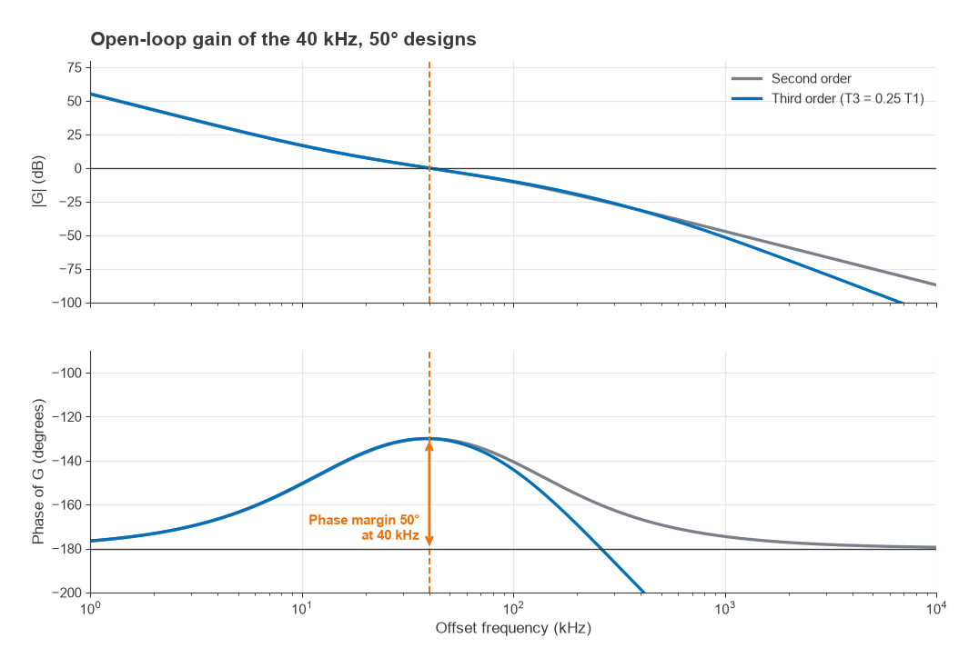
Second-order design: sec 50° − tan 50° = 1.5557 − 1.1918 = 0.3640, so T1 = 1.448 µs and T2 = 10.93 µs. The zero is at 14.6 kHz and the pole at 109.9 kHz, with 40 kHz at their geometric mean. The capacitance equation gives C1 = 3.00 nF, C2 = 19.65 nF and R2 = 556 Ω.
Third-order design with T3 = 0.25T1: solving for 50° gives T1 = 1.146 µs, T3 = 0.287 µs and T2 = 11.05 µs (zero at 14.4 kHz, poles at 138.8 kHz and 555 kHz). The component equations give the values below.
| Component | Calculated | Standard value |
|---|---|---|
| C1 | 1.19 nF | 1.2 nF |
| C2 | 21.5 nF | 22 nF |
| R2 | 514 Ω | 510 Ω |
| R3 | 910 Ω | 910 Ω |
| C3 | 638 pF | 680 pF |
Evaluating G(jω) with the standard values gives fc = 39.6 kHz and a phase margin of 49.6°, close enough to the target. At the 10 MHz PFD frequency the filter transimpedance falls from 5.30 Ω for the second-order design to 0.365 Ω for the third-order design, so the third pole buys about 23 dB of extra reference-spur attenuation with no change to the loop dynamics near fc. A linear simulation of the closed loop shows a 1 MHz output frequency step settling to within 1 kHz in about 38 µs, with 28 percent overshoot. Large steps can cycle-slip and take longer.
Phase Margin and Closed-Loop Peaking
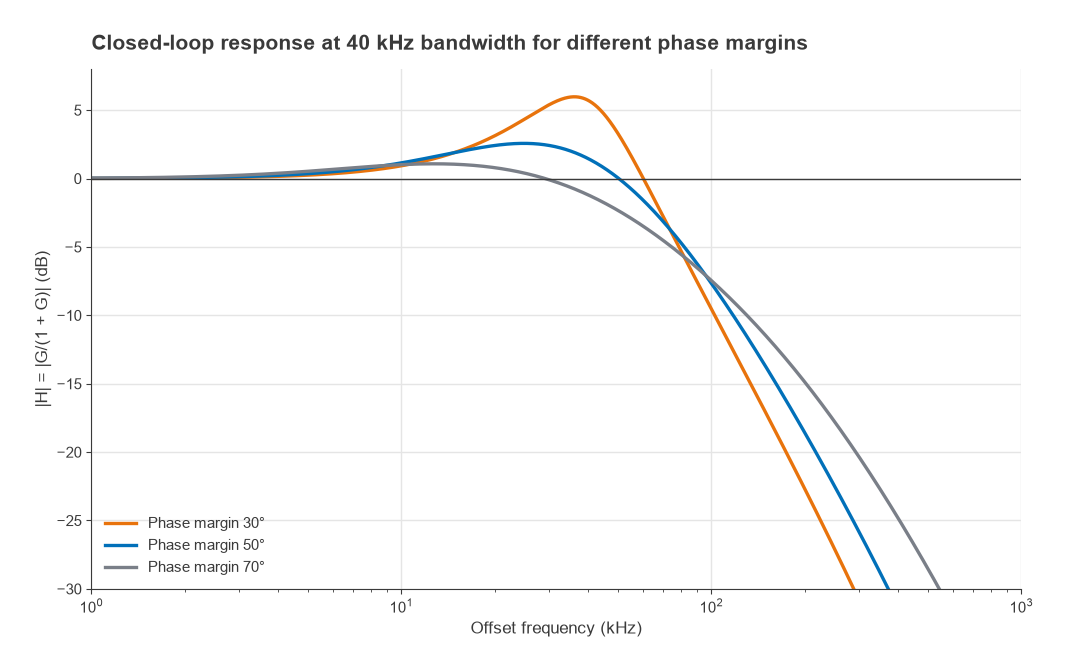
Phase margin trades settling speed against stability and noise peaking. With the same 40 kHz crossover, the third-order design peaks by 6.0 dB at 30° margin, 3.2 dB at 45°, 2.6 dB at 50°, 1.7 dB at 60° and 1.1 dB at 70°. Peaking amplifies in-band noise near the loop bandwidth, and low margins ring longer after a frequency step. Most designs use 45° to 60°.
KVCO often varies by a factor of two across the tuning range, and fc scales roughly with it, so design at the midpoint, check both ends, and adjust the charge pump current where the PLL IC allows.
Loop Bandwidth vs Phase Noise
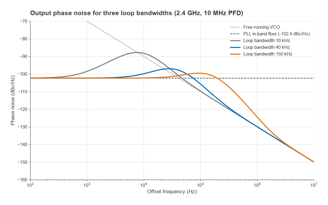
Inside the loop bandwidth the output follows the reference and the PLL’s own noise, multiplied by N. Outside it the output follows the free-running VCO. The in-band floor of a PLL IC is often estimated from a normalized figure of merit:
Lin-band ≈ FOM + 10log10(fPFD) + 20log10(N)
Assuming FOM = −220 dBc/Hz, a value representative of many modern integer-N parts, the example gives −220 + 70 + 47.6 = −102.4 dBc/Hz. If the VCO is −110 dBc/Hz at 100 kHz offset and falls at 20 dB per decade, the two curves cross at 100 kHz × 10(−110 + 102.4)/20 = 41.7 kHz. Setting the loop bandwidth near this crossover usually minimizes integrated phase noise. Integrating the modelled output from 1 kHz to 10 MHz confirms it:
| Loop bandwidth | Phase noise at 10 kHz | at 100 kHz | Integrated (1 kHz to 10 MHz) | RMS jitter at 2.4 GHz |
|---|---|---|---|---|
| 10 kHz | −88.3 dBc/Hz | −109.8 dBc/Hz | 0.42° rms | 485 fs |
| 40 kHz | −99.9 dBc/Hz | −105.7 dBc/Hz | 0.28° rms | 327 fs |
| 150 kHz | −102.3 dBc/Hz | −99.6 dBc/Hz | 0.39° rms | 456 fs |
A narrow loop lets VCO noise through close to the carrier; a wide loop passes the PLL floor out to offsets where the VCO would have been quieter. The model ignores resistor thermal noise, reference noise and PLL 1/f noise, which a full simulation should include. EVM depends on integrated noise, while reciprocal mixing depends on the noise at the offset of the nearest blocker. Measured results can be checked as described in phase noise measurement.
Practical Design Checklist
- Keep fc below roughly fPFD/10; the continuous-time analysis becomes inaccurate closer to the PFD rate.
- Prefer C0G/NP0 or film capacitors; high-K ceramics change value with bias and temperature and some are microphonic.
- A passive filter cannot drive the VCO beyond the charge pump supply; use an active filter when the tuning range needs more.
- Keep the high-impedance tuning node short and away from digital lines.
Frequently Asked Questions
How do you design a PLL loop filter?
Choose the loop bandwidth and phase margin, compute the zero and pole time constants so maximum phase lead falls at the bandwidth, then solve for the capacitance that makes the open-loop gain equal to one there. Divide that into C1, C2 and R2 (plus R3 and C3 for a third-order filter), round to standard values and recheck the margin.
What phase margin should a PLL have?
Between about 45° and 60° is typical. Below about 40° the closed-loop response peaks by several decibels and settling rings; above about 70° the loop gets slower for the same bandwidth.
How wide should the loop bandwidth be?
For lowest integrated phase noise, near the offset where the PLL in-band noise equals the free-running VCO noise. Lock time pushes it wider; spur suppression pushes it narrower.
When is a third-order filter needed?
When reference spurs from the second-order design are too high. The extra RC pole, typically placed four to five times above the main pole, attenuates ripple at the PFD frequency.
Related Topics
See the oscillators and frequency synthesis hub for the full section. PLL frequency synthesis covers the architecture, VCO design the oscillator inside the loop, crystal oscillators the reference, and direct digital synthesis an alternative way to generate fine frequency steps. Phase noise explains the units used here, and frequency planning covers where spurs land in a system.