

Direct digital synthesis (DDS) is a frequency synthesis method that generates a sine wave digitally. A phase accumulator advances by a programmable tuning word on every clock cycle, a lookup table converts the phase to amplitude, and a DAC turns the samples into an analog waveform. Unlike a PLL, it has no feedback loop, so it can change frequency in a single clock cycle with sub-hertz resolution.
The price is a spectrum that is never perfectly clean. Phase truncation, amplitude quantization and DAC nonlinearity produce spurs, the DAC’s zero-order hold imposes a sinc-shaped roll-off, and images of the output appear around every multiple of the clock. This page explains how each part of a DDS works, derives the frequency and spur formulas, and works through a numerical example. It belongs to the oscillators and frequency synthesis section of the RF design map.
How DDS Works
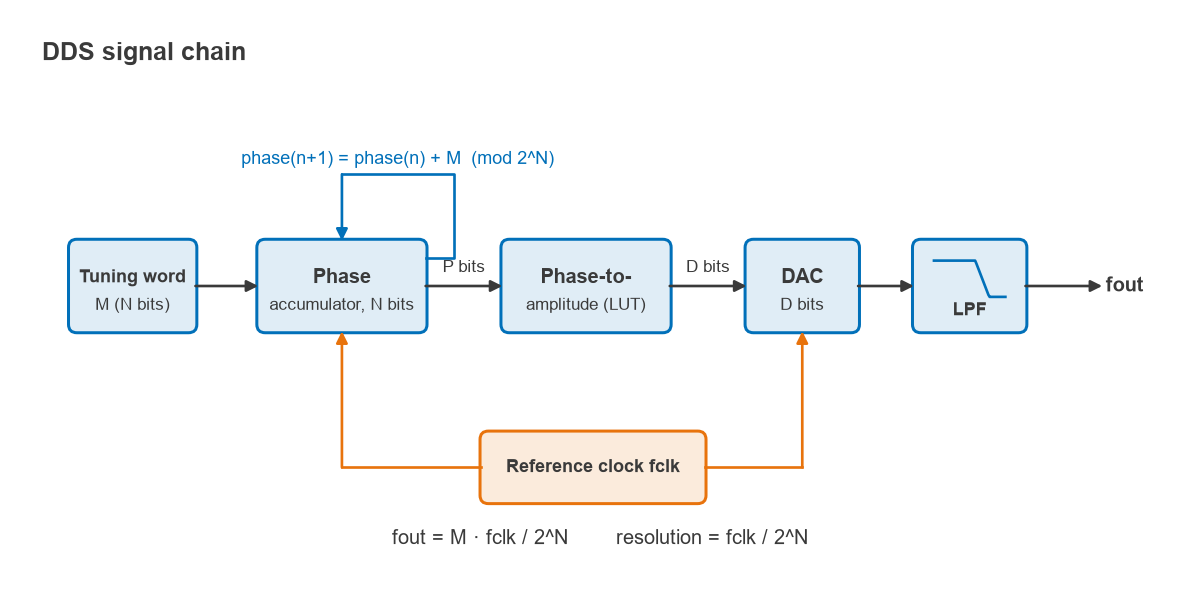
A DDS has four blocks, all clocked by a fixed reference at fclk:
- Phase accumulator: an N-bit register and adder. On each clock edge the tuning word M is added to the register, which wraps around modulo 2N. The register value is the instantaneous phase, with 2N representing one full cycle.
- Phase-to-amplitude converter: the top P bits of the accumulator address a sine lookup table, or drive an equivalent algorithm such as CORDIC. Symmetry lets the table store only a quarter cycle.
- DAC: a D-bit converter turns the amplitude codes into a stepped analog waveform. Its behaviour is covered in Radio Architectures Part 11.
- Reconstruction filter: a low-pass or band-pass filter removes the images above fclk/2 and leaves a smooth sine.
Because the only analog parts are the DAC and filter, the output frequency, phase and amplitude are all set numerically. Many DDS devices add a phase offset register and an amplitude multiplier, which makes phase-coherent switching, PSK and FSK modulation, and linear frequency chirps straightforward.
The Phase Accumulator
The accumulator overflows once every 2N/M clock cycles on average, so the output frequency and resolution are
fout = M · fclk / 2N Δf = fclk / 2N
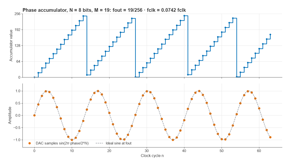
Figure 2 shows a deliberately short 8-bit accumulator with M = 19. The register ramps up in steps of 19 and wraps at 256, giving fout = 19/256 × fclk = 0.0742 fclk. The wrap points do not fall at the same place in each cycle, because 256 is not a multiple of 19. The sine samples are still exact points on the ideal waveform; only the phase at which each sample is taken varies.
Worked Example: Tuning Word and Resolution
A DDS with a 32-bit accumulator and a 1 GHz clock has a resolution of 109/232 = 0.233 Hz. To generate 100 MHz:
- Exact tuning word: 100 × 106 × 232 / 109 = 429,496,729.6.
- Rounded tuning word: M = 429,496,730.
- Actual output: 429,496,730 × 109/232 = 100,000,000.093 Hz, an error of 0.093 Hz or about 0.9 parts per billion.
The frequency accuracy of the output is otherwise that of the clock. A clock derived from a TCXO or OCXO carries its fractional error straight through to fout.
Nyquist limits the output to below fclk/2. In practice the usable range is often taken as up to about 40 % of fclk, so that the reconstruction filter has room to separate the wanted output from the first image at fclk − fout.
Sinc Rolloff and Images
A DAC holds each sample for a full clock period. This zero-order hold multiplies the spectrum of the ideal impulse samples by
H(f) = sin(πf/fclk) / (πf/fclk)
The wanted output therefore drops as its frequency rises: by 0.14 dB at 0.1 fclk, 0.91 dB at 0.25 fclk and 2.42 dB at 0.4 fclk. A DDS swept across its band shows this as a gentle amplitude tilt, which can be corrected digitally with an inverse-sinc filter or by scaling the amplitude word.
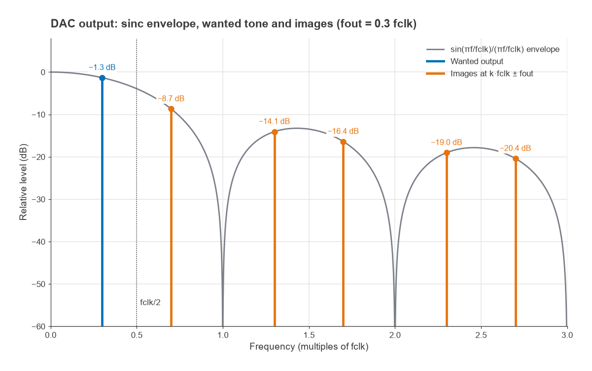
The sampled waveform also contains images at k·fclk ± fout for every integer k, weighted by the same sinc envelope, with nulls at multiples of fclk. In Figure 3, with fout = 0.3 fclk, the wanted tone is at −1.3 dB and the first image at 0.7 fclk is only 7.4 dB below it at −8.7 dB. The reconstruction filter must remove that image to the required spurious level. With a 1 GHz clock and a 300 MHz output, the filter has to pass 300 MHz and reject 700 MHz, which typically calls for an elliptic or high-order Chebyshev response from LC filter design.
Images can also be used deliberately. A band-pass filter placed around fclk + fout selects a higher-frequency image, a technique sometimes called super-Nyquist operation. The sinc envelope makes those images weaker, and DAC output structures designed for this mode change the envelope shape, so the available power has to be checked against the DAC’s documented response.
Spurs: Phase Truncation and Amplitude Quantization
The accumulator is typically 32 or 48 bits wide, but a lookup table with 232 entries would be impractical, so only the top P bits address it. Discarding the lower N − P bits introduces a periodic phase error whose pattern repeats with the accumulator. A periodic error produces discrete spurs rather than a noise floor. The worst-case truncation spur is approximately
spurmax ≈ −6.02 · P dBc
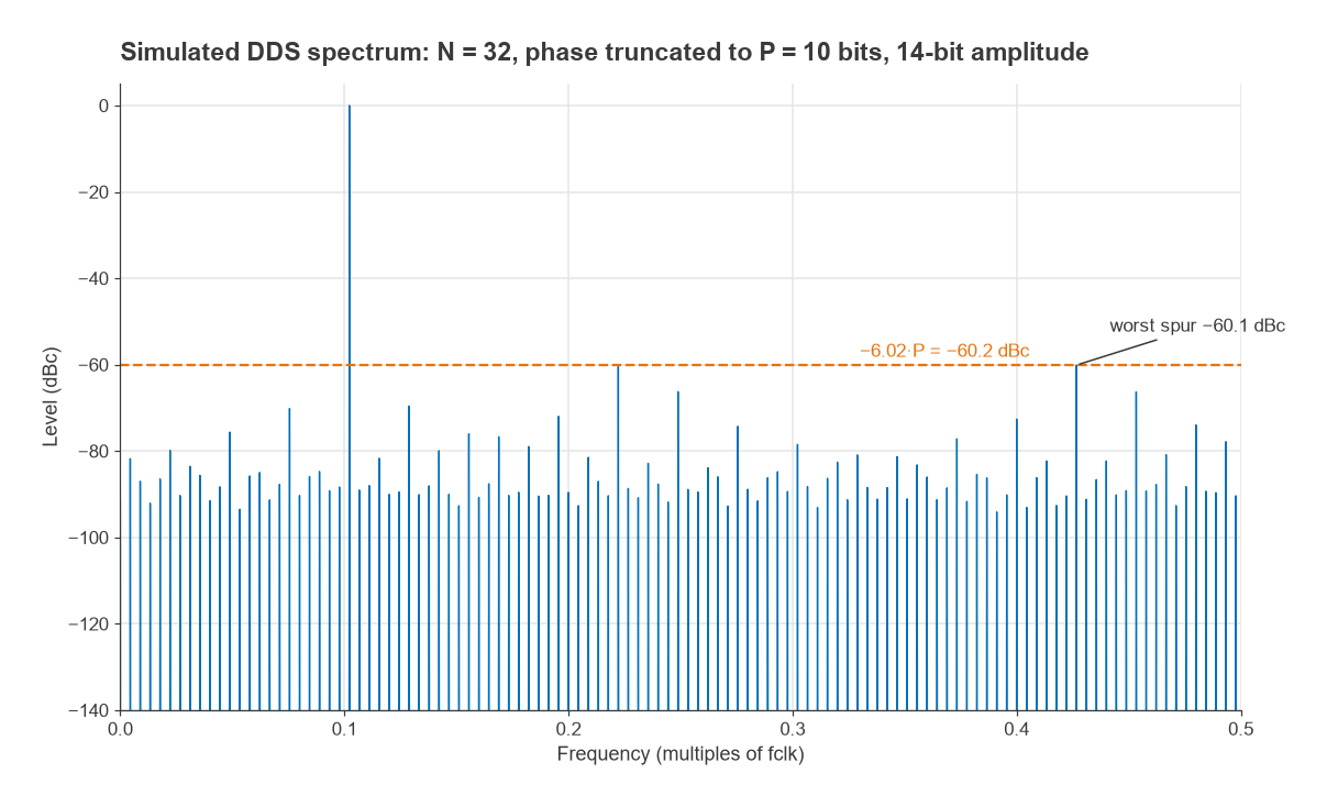
so 12 phase bits give about −72 dBc and 14 bits about −84 dBc. Figure 4 is a simulation with N = 32, P = 10 and a 14-bit amplitude path; the largest spur is −60.1 dBc against a prediction of −60.2 dBc. Whether the spurs appear at all depends on the tuning word: if the lower N − P bits of M are zero, the truncated bits never change and there is no truncation error. Tuning words with many low-order bits set spread the error into many smaller spurs.
Amplitude quantization in the lookup table and DAC behaves more like noise when the output and clock frequencies are unrelated. For an ideal D-bit converter the signal-to-quantization-noise ratio over the Nyquist band is
SQNR = 6.02 D + 1.76 dB
A 12-bit DAC gives 74.0 dB. Spread over the 500 MHz Nyquist band of a 1 GHz clock, that is a noise density of −74.0 − 10 log(5 × 10⁸) = −161.0 dBc/Hz. When fout is a simple fraction of fclk, the quantization error becomes periodic and concentrates into spurs instead.
DAC Harmonics and Aliasing
In practice the largest spurs usually come from DAC nonlinearity rather than truncation. Harmonics of fout are generated in the DAC and fold back into the first Nyquist zone. With fclk = 1 GHz and fout = 300 MHz:
| Harmonic | Unaliased frequency (MHz) | Appears at (MHz) |
|---|---|---|
| 2nd | 600 | 400 |
| 3rd | 900 | 100 |
| 4th | 1200 | 200 |
| 5th | 1500 | 500 |
The third harmonic lands at 100 MHz, well inside the passband of any filter that passes 300 MHz, so it cannot be filtered out. The usual remedy is frequency planning: choose fclk and the output range so that low-order harmonics alias away from the band of interest. Spur levels from DAC nonlinearity depend on the specific converter and are given in its data sheet as SFDR versus output frequency.
Phase Noise of a DDS
A DDS behaves like a fractional frequency divider. The clock’s phase noise is reduced at the output by
Lout(Δf) = Lclk(Δf) − 20 log(fclk/fout)
A 1 GHz clock with −140 dBc/Hz at some offset would, in principle, give −160 dBc/Hz at the same offset on a 100 MHz output. The improvement stops at the residual phase noise of the DDS itself, set by jitter in the DAC clocking and its digital logic, and at the quantization noise floor. Low-frequency outputs therefore often hit the residual floor rather than the scaled clock noise.
DDS Compared with a PLL
A PLL synthesizer multiplies a reference up to microwave frequencies using a VCO, with spurs and noise shaped by the loop filter. Its switching time is limited by the loop bandwidth, typically microseconds or longer. A DDS is limited to below half its clock but switches in nanoseconds, has fine resolution without fractional-N techniques, and can switch phase-continuously. The two are often combined: a DDS can serve as a finely tunable reference for a PLL, or a DDS output can be mixed with a fixed PLL to translate it upward. Chirp generation for radar, agile local oscillators and test sources are common uses.
Frequently Asked Questions
How does DDS work?
A phase accumulator adds a tuning word to itself every clock cycle, producing a ramp that wraps around once per output cycle. A lookup table converts the phase to sine amplitude, and a DAC and reconstruction filter turn the samples into an analog sine at M · fclk/2N.
What causes spurs in a DDS?
Truncating the accumulator phase to P bits produces spurs up to about −6.02P dBc. Amplitude quantization adds noise or spurs, and DAC nonlinearity produces harmonics that alias into the first Nyquist zone. In practical devices the DAC harmonics are usually the largest.
Why does DDS output amplitude fall with frequency?
The DAC holds each sample for a full clock period, which multiplies the spectrum by sin(πf/fclk)/(πf/fclk). The loss is 2.42 dB at 40 % of the clock frequency and grows toward the Nyquist frequency.
What is the maximum output frequency of a DDS?
The theoretical limit is fclk/2. A common practical limit is about 40 % of fclk, leaving a transition band for the reconstruction filter. Higher Nyquist zones can be used with a band-pass filter at reduced output level.
Related Topics
For other synthesis methods see PLL frequency synthesis and VCO design. The DAC behind the DDS output is covered in DACs in the transmit chain, and spur avoidance in frequency planning. The oscillators hub lists every topic in this section, and the wireless terms glossary defines the abbreviations used here.