

Biasing an RF amplifier means supplying the DC voltage and current that set the transistor’s operating point while keeping the bias network invisible to the RF signal. A single-pin Darlington MMIC is usually biased by feeding a supply through a series resistor and an RF choke into its output pin, with blocking capacitors on the RF ports. The resistor sets the current, and the choke stops the supply from loading the RF path.
The same building blocks, a DC feed inductor, a DC blocking capacitor and decoupling to ground, make up the bias tee used to power remote amplifiers over coaxial cable. Discrete transistors add gate or base bias, and active bias circuits hold the current constant against temperature, supply and part-to-part variation. This page covers resistor bias for MMICs, choke and bias tee design, active bias and FET bias sequencing, with worked component values. It belongs to the RF amplifiers section of the RF design reference.
What a bias network has to do
A bias network has four jobs. It sets the quiescent current and voltage that determine gain, noise figure, linearity and efficiency. It holds that operating point steady as temperature, supply voltage and device parameters vary. It presents a high impedance to the RF path across the whole band, so that no signal is lost into the supply. And it presents a low impedance to ground at the supply side, at RF and at the lower frequencies where a transistor still has gain, so that the amplifier remains stable. The last point is often missed: a transistor with a poorly decoupled bias line can oscillate at a frequency far below the operating band.
Resistor and choke bias for Darlington MMICs
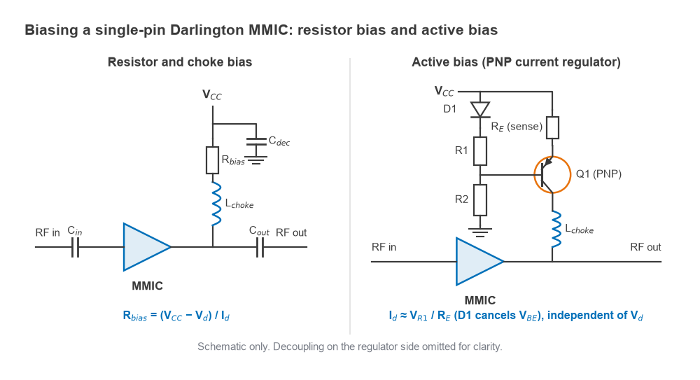
A Darlington gain block of the kind described in broadband RF amplifier design has a single pin that is both the RF output and the DC supply. Its datasheet specifies a device voltage Vd at a recommended current Id. The device behaves roughly like a voltage source of Vd, so it must be fed from a current-limited supply. The simplest way is a resistor from a higher supply VCC:
Rbias = (VCC − Vd) / Id
An RF choke between the resistor and the output pin isolates the RF signal from the resistor and supply. A decoupling capacitor at the supply side of the resistor shorts any residual RF to ground. Blocking capacitors on the input and output keep DC out of the neighbouring stages.
Worked example: a 5 V, 65 mA gain block on a 12 V rail
- Rbias = (12 − 5)/0.065 = 107.7 Ω. The nearest E24 value, 110 Ω, gives Id = 7/110 = 63.6 mA, close enough to the recommended current.
- Resistor dissipation: 0.06362 × 110 = 0.445 W. A 1 W part, or two 220 Ω resistors in parallel at 0.22 W each, gives margin.
- Device dissipation: 5 × 0.0636 = 0.318 W. Total supply power is 0.764 W, of which 58% is dropped in the resistor.
- Choke: for a band starting at 50 MHz, aim for a choke reactance of about ten times Z0, 500 Ω. L = 500/(2π × 50×106) = 1.59 µH. Check that the choke has no low-impedance resonance anywhere in the band (see below).
- Blocking capacitors: a reactance of Z0/10 = 5 Ω at 50 MHz needs C = 1/(2π × 50×106 × 5) = 637 pF. A 1 nF capacitor is a common choice, provided its self-resonance and package inductance are acceptable at the top of the band.
- Decoupling: a 100 nF capacitor has 0.032 Ω reactance at 50 MHz. In practice a small RF capacitor in parallel with a larger bulk capacitor covers both RF and low frequencies, as described in RF power supply decoupling.
Why supply headroom matters
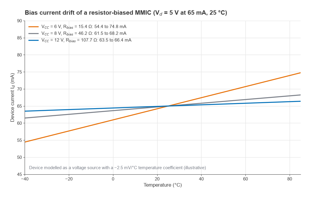
Vd of a Darlington typically falls as temperature rises, by a few millivolts per degree. With resistor bias, any change in Vd or VCC appears across Rbias, so a larger resistor, which needs a higher supply, gives a more stable current. Figure 2 uses an illustrative coefficient of −2.5 mV/°C over −40 to +85 °C:
| VCC | Rbias | Resistor power | Current change, −40 to +85 °C | Current change, ±5% supply |
|---|---|---|---|---|
| 6 V | 15.4 Ω | 0.065 W | 20.3 mA (31%) | ±19.5 mA (30%) |
| 8 V | 46.2 Ω | 0.195 W | 6.8 mA (10%) | ±8.7 mA (13%) |
| 12 V | 107.7 Ω | 0.455 W | 2.9 mA (4.5%) | ±5.6 mA (8.6%) |
The trade is efficiency against stability. With only 1 V of headroom, the current swings by almost a third, which shifts gain and P1dB and, at the hot end, can push the device past its rated current. Many datasheets recommend a minimum resistor or minimum headroom for this reason. Where the supply is too low for adequate headroom, active bias is the better answer.
RF chokes and their resonances
A real inductor has parasitic capacitance between turns, so it resonates at its self-resonant frequency (SRF) and behaves as a capacitor above it. The parasitic models are covered in RF component parasitics. A 1.5 µH chip inductor with 0.30 pF of parasitic capacitance resonates at 237 MHz. Above that its impedance falls: about 560 Ω at 1 GHz and 180 Ω at 3 GHz. For a narrow band that is fine. For a broadband amplifier, no single inductor is large enough at the low end and still high in impedance at the top.
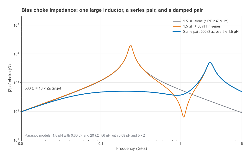
The usual fix is a small, high-SRF inductor next to the RF line in series with a large inductor further away. That introduces a new problem, shown in Figure 3. Above its SRF the large inductor is capacitive, and that capacitance series-resonates with the small inductor. With a 56 nH inductor (0.08 pF, SRF 2.38 GHz) in series with the 1.5 µH part, the combined impedance drops to 62 Ω at 1.11 GHz. Shunting a matched 50 Ω line, that dip causes up to 2.93 dB of loss, a deep notch in the gain. A 500 Ω resistor across the large inductor damps the resonance: the combined impedance then stays above 358 Ω from 50 MHz to 6 GHz, and the worst-case shunt loss falls to 0.56 dB. The damping lowers the peak impedance, so the resistor value is a compromise. Conical inductors, which have a wide range between their low-frequency inductance and their SRF, are the usual choice for multi-octave bias feeds up to microwave frequencies.
Bias tee design
A bias tee is a three-port network with an RF port, a DC port and a combined RF+DC port. It contains a series blocking capacitor between the RF and combined ports and a choke between the DC and combined ports, with decoupling on the DC side. The resistor-and-choke MMIC feed above is a bias tee built into the amplifier layout. Stand-alone bias tees are used to inject DC onto a coaxial cable, for example to power a mast-mounted amplifier from the receiver end, as in the LNA for SDR guide, or to bias a device under test on a VNA.
Design starts from the lowest frequency, fL. The capacitor reactance should be small compared with Z0 and the choke reactance large compared with Z0, with Z0/10 and 10Z0 as common starting rules:
C ≥ 10 / (2πfLZ0), L ≥ 10Z0 / (2πfL)
The upper frequency is set by the SRF of the capacitor and the impedance of the choke, as discussed above. Two further checks matter. The DC current must stay below the choke’s rated current, or its inductance falls as the core saturates. And the capacitor must withstand the DC voltage plus the RF peak. A bias tee feeding a cable should also tolerate a shorted cable.
Active bias circuits
An active bias circuit replaces the dropping resistor with a transistor that regulates the current. In the common PNP form, a sense resistor RE sits between the supply and the PNP emitter. A divider of R1 and R2 sets the base voltage, with a diode D1 in series with R1 so that its forward voltage cancels the PNP’s VBE and its temperature drift. The voltage across RE then equals the voltage across R1, and
Id ≈ VR1 / RE
For the same 65 mA device on 12 V, choose 1.0 V across RE: RE = 1.0/0.065 = 15.4 Ω. With 10 mA in the divider, about fifteen times the 0.65 mA base current of a transistor with a current gain of 100, R1 = 1.0/0.010 = 100 Ω. The base sits at 12 − 1.0 − 0.65 = 10.35 V, so R2 ≈ 10.35/0.010 = 1.04 kΩ, rounded to 1.0 kΩ. The device can now have any Vd up to about 10.7 V, leaving 0.3 V across the PNP, and its current no longer depends on Vd. The only dissipating parts are RE (65 mW) and the PNP (0.39 W at Vd = 5 V). Integrated active bias controllers do the same job with a reference and an error amplifier and can also generate negative gate voltages.
The regulating loop must not have gain at RF or at low frequencies where it could interact with the amplifier. A decoupling capacitor at the PNP base and at the collector side of the choke keeps the loop slow and the RF out of it.
Biasing discrete transistors and FETs
Discrete bipolar stages are biased with a base feed and a collector feed, each through a choke or a quarter-wave line, with emitter degeneration or a collector-to-base feedback resistor to stabilise the current against β and temperature. Enhancement-mode FETs need a positive gate voltage and depletion-mode devices, including most GaAs pHEMTs and GaN HEMTs, need a negative gate voltage to pinch off the channel. The gate draws very little current, so a high-value resistor in the gate feed both isolates the RF and helps low-frequency stability.
Depletion-mode devices require bias sequencing. If the drain supply is applied while the gate is at 0 V, the device conducts its maximum current and can be destroyed. The safe order is: apply the negative gate voltage, apply the drain voltage, then adjust the gate to the target drain current. Power-down reverses the order. Sequencing circuits or bias controllers enforce this automatically. The transistor families and their bias needs are compared in RF transistor technologies, and high-power bias networks interact with heat flow as described in RF PA thermal design.
Frequently asked questions
How do you bias an MMIC amplifier?
For a single-pin Darlington MMIC, feed the output pin from a higher supply through a resistor Rbias = (VCC − Vd)/Id and an RF choke, decouple the supply side, and add DC blocking capacitors on the RF ports. Use enough supply headroom that temperature and supply changes do not move the current too far, or use an active bias circuit.
What is a bias tee?
A bias tee is a three-port network that combines DC and RF on one port. A series capacitor passes RF and blocks DC, and a choke passes DC and blocks RF. It is used to power amplifiers over coaxial cable and to bias devices during measurement.
How large should an RF choke be?
A common starting point is a reactance of about ten times the line impedance at the lowest frequency, 500 Ω in a 50 Ω system, which is 1.59 µH at 50 MHz. The choke must also avoid low-impedance resonances across the band, which is why broadband feeds use conical inductors or damped series combinations.
Why does a GaN or GaAs FET need bias sequencing?
Depletion-mode FETs conduct heavily at zero gate voltage. Applying drain voltage before the negative gate bias can drive the device to destructive current. The gate is always applied first and removed last.
Related topics
Bias design connects to broadband amplifier design, LNA design and power amplifier design and load-pull. For component and layout effects see RF component parasitics and power supply decoupling. The section index is RF amplifiers, and terms are defined in the wireless terms glossary.