

Skin effect is the tendency of alternating current to flow in a thin layer near the surface of a conductor, with current density falling exponentially with depth. The characteristic thickness of that layer, the skin depth, shrinks as the square root of frequency, so at RF the effective cross-section of a conductor is far smaller than its physical one and its resistance is correspondingly higher.
For copper the skin depth is about 65 µm at 1 MHz and about 2.1 µm at 1 GHz. That is why conductor loss in transmission lines, inductors and connectors rises with frequency, why plating and surface finish matter, and why copper roughness becomes a design parameter in microwave circuit boards. This page derives the skin depth formula, shows how to compute surface resistance and conductor loss, and explains the effect of surface roughness, with worked examples. It belongs to the RF fundamentals section of the RF design guide.
Why Current Crowds to the Surface
A time-varying current produces a time-varying magnetic field inside the conductor. By Faraday’s law that field induces circulating eddy currents which oppose the original current in the interior and reinforce it near the surface. The deeper a filament of current lies, the more flux it links and the higher its inductance, so the current redistributes toward the surface where the impedance is lowest. The faster the field changes, the stronger the effect.
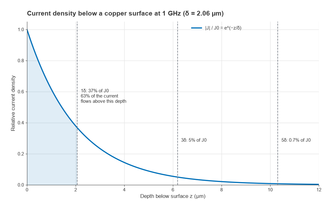
Solving Maxwell’s equations for a good conductor, where conduction current dominates displacement current, gives a field that decays and changes phase with depth z below a flat surface:
J(z) = J0 e−z/δ e−jz/δ
The magnitude falls to 1/e, about 37%, at one skin depth. Integrating the current density shows that 63% of the total current flows within the first skin depth and 95% within three. Because dissipated power goes as |J|2, about 86% of the loss occurs within one skin depth and 99.75% within three. The same decay governs how electromagnetic waves penetrate any good conductor, which is the basis of shielding.
How to Calculate Skin Depth
The skin depth is
δ = √(ρ / (π f μ)) = 1 / √(π f μ σ)
where ρ is the resistivity in Ω·m, σ = 1/ρ the conductivity, f the frequency in Hz and μ = μ0μr the permeability, with μ0 = 4π × 10−7 H/m. For non-magnetic metals μr = 1.
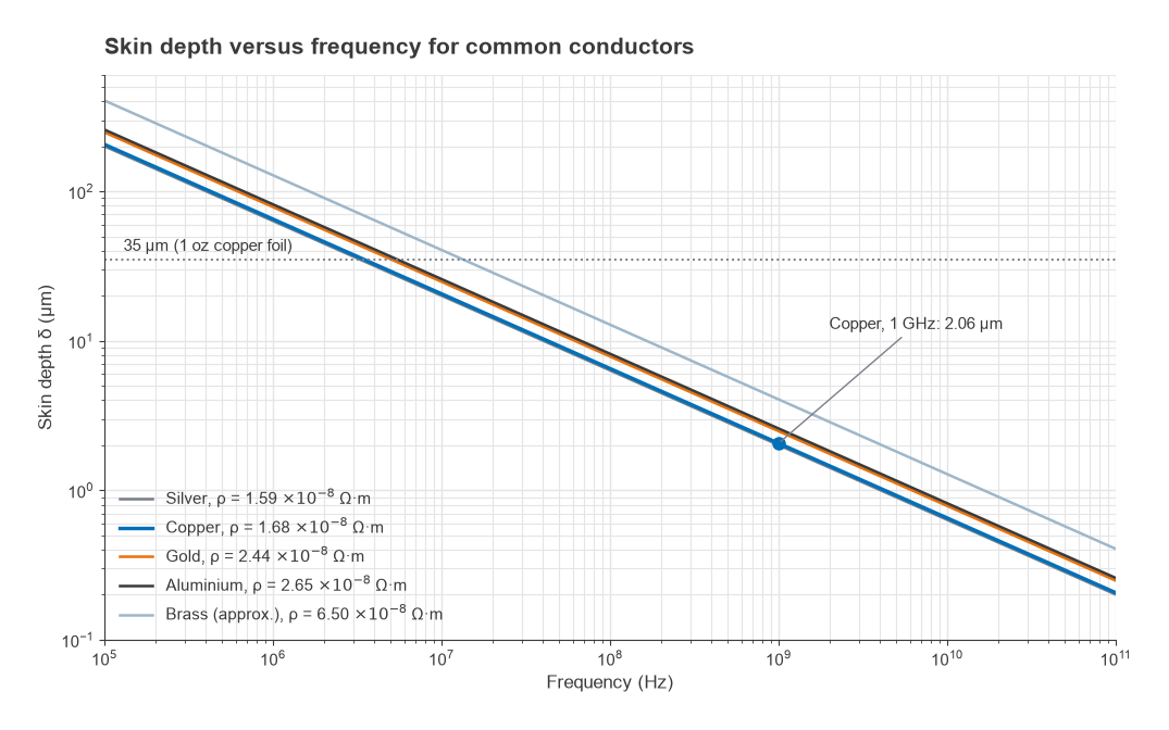
Worked example: copper at 1 GHz
Annealed copper has ρ ≈ 1.68 × 10⁻⁸ Ω·m at room temperature. At 1 GHz:
δ = √(1.68 × 10⁻⁸ / (π × 109 × 4π × 10−7)) = √(4.26 × 10⁻¹²) = 2.06 µm
Since δ scales as 1/√f, a decade in frequency changes it by √10 ≈ 3.16. Copper therefore has δ ≈ 6.52 µm at 100 MHz and 0.65 µm at 10 GHz. The table gives values for other common conductors using typical room-temperature resistivities; alloy resistivities, brass in particular, vary with composition, so treat those as approximate.
| Metal | ρ (10−8 Ω·m) | δ at 1 MHz | δ at 100 MHz | δ at 1 GHz | δ at 10 GHz |
|---|---|---|---|---|---|
| Silver | 1.59 | 63.5 µm | 6.35 µm | 2.01 µm | 0.63 µm |
| Copper | 1.68 | 65.2 µm | 6.52 µm | 2.06 µm | 0.65 µm |
| Gold | 2.44 | 78.6 µm | 7.86 µm | 2.49 µm | 0.79 µm |
| Aluminium | 2.65 | 81.9 µm | 8.19 µm | 2.59 µm | 0.82 µm |
| Brass (approx.) | 6.5 | 128 µm | 12.8 µm | 4.06 µm | 1.28 µm |
The frequency to skin depth relationship is analogous to the frequency and wavelength relationship in that it sets a physical length scale that a designer must compare with the geometry, here conductor thickness rather than circuit size.
Surface Resistance and Conductor Loss
When a conductor is many skin depths thick, the exponential current distribution behaves exactly like a uniform current in a layer one skin depth thick. The resistance of a square of surface, the surface resistance, is therefore
Rs = ρ/δ = √(π f μ ρ) (Ω per square)
For copper, Rs = 8.1 mΩ at 1 GHz and 25.8 mΩ at 10 GHz. Conductor loss therefore rises as √f, while dielectric loss rises roughly in proportion to f, which is why conductor loss dominates in many lines at low frequencies and dielectric loss takes over at higher ones on lossy laminates. The general treatment of line loss is in transmission line losses.
Worked example: AC resistance of a round wire
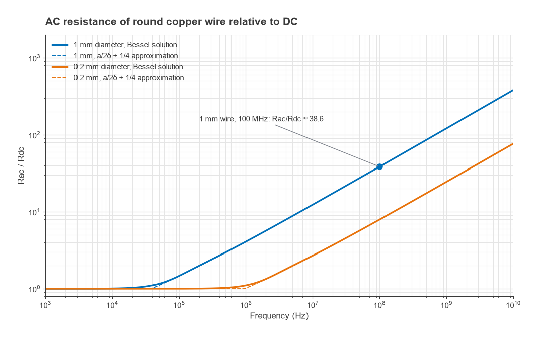
A copper wire of diameter d = 1 mm has a DC resistance of ρ/(πd2/4) = 21.4 mΩ per metre. At 100 MHz, with δ = 6.52 µm much smaller than the radius, the current flows in an annulus of circumference πd and thickness δ:
Rac ≈ ρ/(π d δ) = 1.68 × 10⁻⁸ / (π × 10−3 × 6.52 × 10−6) = 0.82 Ω per metre
That is about 38 times the DC value. The exact solution for a round wire uses Bessel functions and gives 38.6 at this frequency; the simple annulus formula is within 1% here, and the refinement Rac/Rdc ≈ a/(2δ) + 1/4, with a the radius, comes within 0.1%. Higher resistance lowers the Q of inductors and resonators built from wire or traces, which ties skin effect directly to Q factor and to the parasitic resistance of RF components.
Worked example: microstrip conductor loss
A first estimate of conductor attenuation for a wide microstrip is αc ≈ Rs/(Z0W) nepers per metre. For a 50 Ω line 1.1 mm wide on a thin low-loss laminate at 10 GHz, αc ≈ 0.0258/(50 × 0.0011) = 0.47 Np/m, which is 4.1 dB/m or about 0.04 dB/cm with perfectly smooth copper. The estimate ignores current crowding at the strip edges and the finite ground plane current distribution, so a field solver will usually give a somewhat higher value. The microstrip calculator gives the line width for a given substrate.
Surface Roughness and Loss
Copper foil for circuit boards is deliberately roughened on the side bonded to the dielectric so that it adheres well. Once the skin depth becomes comparable with the height of that roughness, current has to follow the bumps and valleys, the path length increases and so does the loss. At 10 GHz the copper skin depth is 0.65 µm, which is smaller than the profile of many standard foils.
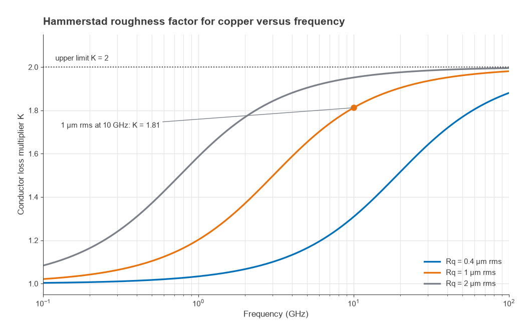
The classic empirical correction, usually attributed to Hammerstad and Jensen, multiplies the smooth-conductor loss by
K = 1 + (2/π) arctan(1.4 (Rq/δ)2)
where Rq is the rms surface roughness. K tends to 1 when the surface is smooth compared with δ and saturates at 2 when it is very rough. For Rq = 1 µm at 10 GHz, (Rq/δ)2 = 2.35 and K = 1.81, so the microstrip example above rises from 4.1 to about 7.4 dB/m. A smoother foil with Rq = 0.4 µm gives K = 1.31 and about 5.3 dB/m.
Measurements on modern foils at millimetre-wave frequencies often show loss rising beyond the factor of 2 that the Hammerstad model allows. Models based on the shape of the copper nodules, such as the Huray “snowball” model, and gradient conductivity models fit those cases better and are built into many EM solvers. In practice, laminate and foil choice is made together, as discussed in FR-4 vs Rogers, and the roughness value should come from the laminate or foil supplier’s data for the specific foil type.
Design Consequences
Conductor and plating thickness
A conductor needs to be several skin depths thick to reach its full-thickness surface resistance; three to five skin depths is a common rule. One-ounce copper, about 35 µm, is roughly 17 skin depths at 1 GHz, and five skin depths down to about 87 MHz, so thickness rarely limits copper loss on RF boards. Plating is different. A thin gold or silver layer over another metal carries most of the current only if it is several skin depths thick at the operating frequency; otherwise much of the current flows in the underlying metal.
Magnetic metals and nickel barriers
Ferromagnetic metals have μr greater than 1, which shrinks the skin depth and raises Rs by √μr. Nickel is used as a barrier layer under gold in some surface finishes. Its effective permeability at RF depends strongly on frequency and on the deposit, and it tends to fall at microwave frequencies, but where it is significant the current confined in the nickel layer adds measurable loss. As an illustration only, nickel with an assumed μr of 100 would have a skin depth near 0.4 µm at 1 GHz, against about 4.2 µm if it were non-magnetic. Low-loss designs often choose finishes without a nickel layer on RF traces.
Proximity effect, litz wire and waveguides
Nearby conductors carrying current push each other’s current to the facing or opposite sides, the proximity effect, which further raises the resistance of closely wound coils. At lower frequencies, roughly up to the low MHz range, litz wire made of many insulated strands reduces both effects; at VHF and above the strands become comparable with δ and the benefit fades. The same skin-depth arithmetic sets the wall loss of waveguides and cavities, which is why high-Q cavities are often silver plated.
Frequently Asked Questions
What is skin effect?
It is the concentration of alternating current near the surface of a conductor, caused by eddy currents induced by the conductor’s own magnetic field. Current density falls exponentially with depth, so the conductor behaves as if only a thin surface layer carried current, which raises its resistance at high frequencies.
How do you calculate skin depth?
Use δ = √(ρ/(πfμ)). For copper with ρ = 1.68 × 10⁻⁸ Ω·m and μ = μ0, this gives 2.06 µm at 1 GHz. Skin depth scales as 1/√f, so it falls by a factor of 3.16 for each decade of frequency.
How does surface roughness affect loss?
When the rms roughness is comparable with the skin depth, current follows the surface profile and loss increases. The Hammerstad model gives a multiplier between 1 and 2; for 1 µm rms copper at 10 GHz it is about 1.8. Smooth foils reduce this penalty.
How thick should an RF conductor be?
At least three to five skin depths at the lowest frequency of interest. Standard 35 µm copper meets this for most RF work above about 100 MHz, but thin platings may not.
Related Topics
The RF fundamentals hub links the other basics, including dB and dBm and frequency bands. For lines and boards see transmission line parameters and RF PCB layout. Terms are defined in the wireless terms glossary.