

A distributed amplifier, also called a traveling-wave amplifier, is a broadband amplifier in which several transistors are connected between two artificial transmission lines so that their input and output capacitances become part of the lines instead of limiting bandwidth. The input signal travels down the gate line and drives each transistor in turn, and the output currents add in phase on the drain line as they travel toward the load.
The result is gain that extends from near DC to a large fraction of the transistor cutoff frequency, at the cost of modest gain per device, more die area and lower efficiency than a tuned stage. Distributed amplifiers are the usual choice when an application needs a decade or more of bandwidth, such as instrumentation, optical modulator drivers and wideband receivers. This page explains how the artificial lines work, derives the gain and gain-bandwidth expressions, and works through a four-cell example checked by circuit simulation. It sits in the RF amplifiers section of the RF design guide.
How a Distributed Amplifier Works
In a conventional single-stage amplifier, the input capacitance of the transistor has to be charged through the source resistance, which sets a pole at roughly 1/(2πRsCgs). Adding more transistors in parallel raises the transconductance but raises the capacitance by the same factor, so the gain-bandwidth product stays near the transistor fT. The distributed amplifier breaks this limit by never presenting the capacitances in parallel.
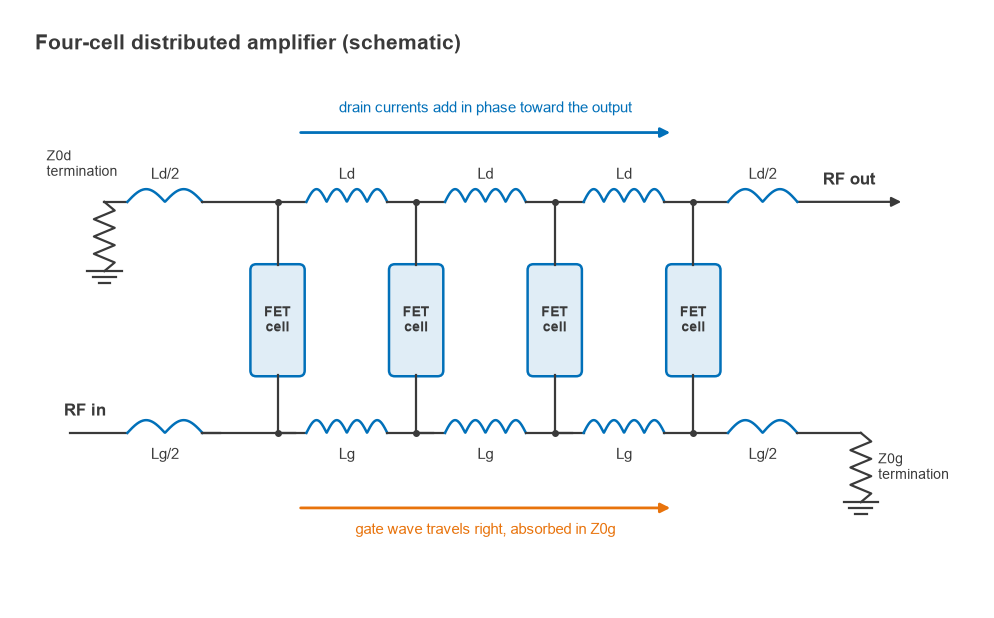
Each transistor gate is connected to a node of a ladder of series inductors. The inductors and the gate-source capacitances together form a lumped approximation of a transmission line, the gate line, terminated at its far end in its characteristic impedance. The drains are connected in the same way to a second ladder, the drain line, which is terminated at its input end and delivers power to the load at its output end.
A signal applied to the gate line travels from cell to cell. Each transistor converts its gate voltage into a drain current, and that current launches two waves on the drain line, one toward the output and one toward the drain termination. If the phase delay per section on the drain line equals that on the gate line, every forward-travelling contribution arrives at the output in phase with the others and they add. The reverse waves do not line up and are absorbed in the drain termination. Whatever signal reaches the end of the gate line is absorbed in the gate termination.
Artificial Transmission Lines
A ladder of series inductors L and shunt capacitors C is a constant-k low-pass filter. Well below its cutoff it behaves like a uniform transmission line with
Z0 = √(L/C) fc = 1/(π√(LC))
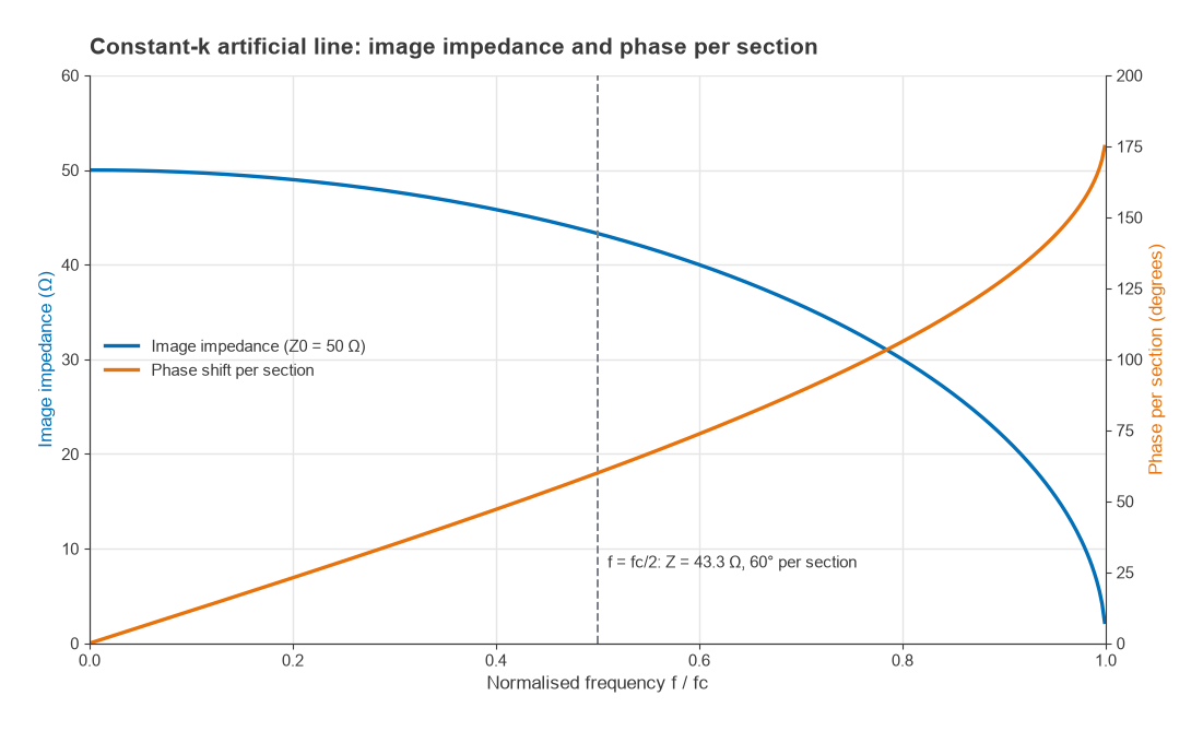
where fc is the cutoff (Bragg) frequency of the ladder. Near cutoff the line is no longer smooth. The image impedance of a mid-shunt section falls as ZI = Z0√(1 − (f/fc)2), and the phase shift per section rises as φ = 2 arcsin(f/fc), reaching 180° at cutoff. A fixed resistive termination therefore matches the line well only up to perhaps half of fc; designers use m-derived end sections to keep the termination closer to the image impedance over more of the band.
On the gate line C is the transistor Cgs. On the drain line C is the drain-source capacitance Cds, which is normally much smaller, so an extra padding capacitor is added at each drain node to equalise the phase velocity of the two lines. With equal Z0 on both lines the condition is simply Cds + Cpad = Cgs. The same ideas underlie ordinary transmission line parameters, and the general theory is in transmission line theory.
Gain of a Distributed Amplifier
For an ideal lossless amplifier with N cells, transconductance gm per cell and gate and drain line impedances Z0g and Z0d, each cell injects gmVin into the drain line, half of which travels toward the load. The output voltage is N gmVinZ0d/2 and the available power gain is
G = gm2 N2 Z0g Z0d / 4
Gain grows as N2 in this limit, which is the main attraction. Real lines have loss. On the gate line the input resistance Ri in series with Cgs absorbs power, and on the drain line the output resistance Rds loads every node. If Ag and Ad are the attenuations per section in nepers, the gain becomes
G = (gm2 Z0g Z0d / 4) × (e−NAg − e−NAd)2 / (e−Ag − e−Ad)2
with the low-frequency approximations Ag ≈ ω2Cgs2RiZ0g/2 and Ad ≈ Z0d/(2Rds). This expression appears in standard microwave texts. It reduces to the lossless form when both attenuations go to zero and to gm2Z02/4 for one cell.
Optimum number of cells
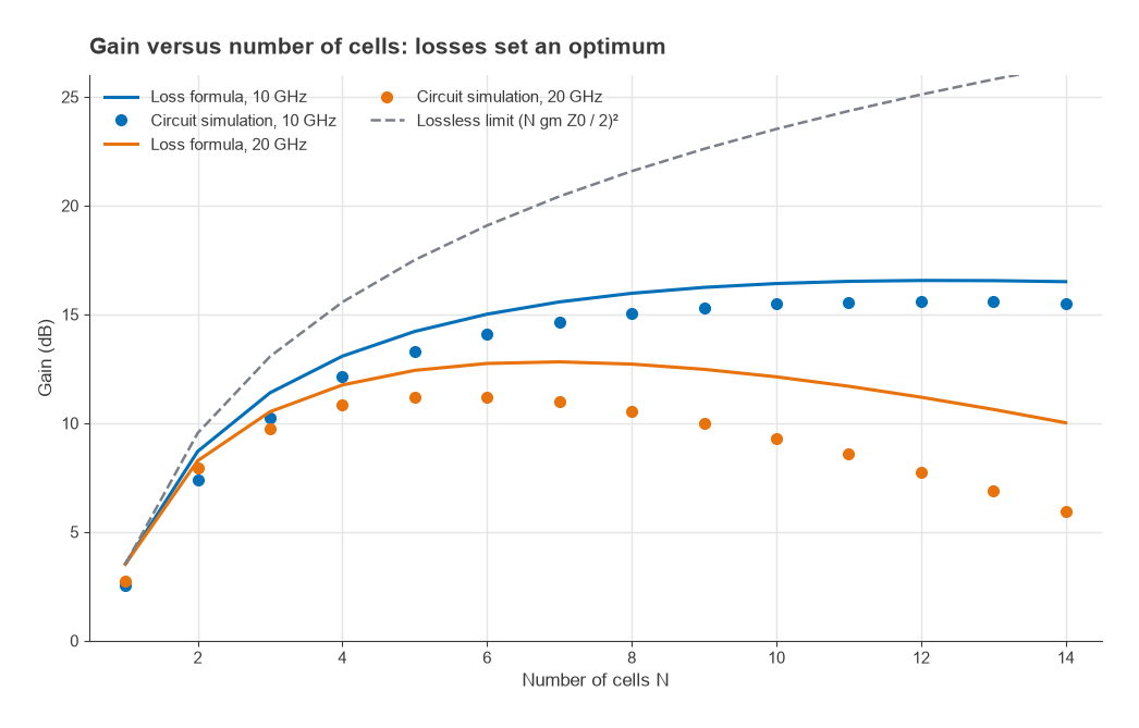
Adding cells adds current to the drain line, but every added section also attenuates the signal already travelling on both lines. Differentiating the lossy gain expression with respect to N gives the optimum
Nopt = ln(Ad/Ag) / (Ad − Ag)
Because Ag rises with the square of frequency, the optimum falls as the top of the band rises. Practical designs commonly use somewhere between three and ten cells; beyond the optimum, extra cells cost area and DC power and reduce gain at the upper band edge.
Gain-Bandwidth of the Distributed Amplifier
With Z0 = √(L/Cgs), the gate line cutoff can be written fc = 1/(πZ0Cgs). The lossless voltage gain is Av = N gmZ0/2. Their product is
Av × fc = N gm / (2πCgs) = N fT
A lumped amplifier built from the same devices is limited to a voltage gain-bandwidth near fT, however many devices are placed in parallel. The distributed amplifier scales it by the number of cells, which is why the topology can reach bandwidths close to the device cutoff while still providing useful gain. Losses reduce the benefit, and the choice of Z0 trades gain against bandwidth: a higher impedance raises gmZ0 but lowers fc for the same Cgs. Device choice matters for the same reason, and the RF transistor technologies page compares fT and output resistance across GaAs, GaN, SiGe and CMOS.
Worked Example: a Four-Cell Design
Take a generic FET cell with gm = 60 mS, Cgs = 0.2 pF, Ri = 8 Ω, Rds = 150 Ω and Cds = 0.05 pF, and design for 50 Ω lines.
- Line inductance: L = Z02Cgs = 2500 × 0.2 pF = 0.5 nH per section, used on both lines.
- Drain padding: Cpad = 0.2 − 0.05 = 0.15 pF per drain node.
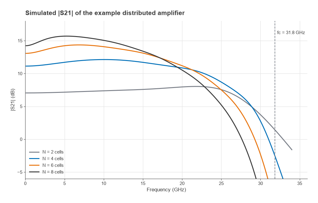
- Line cutoff: fc = 1/(π × 50 × 0.2 pF) = 31.8 GHz.
- Device fT = 0.06/(2π × 0.2 pF) = 47.7 GHz.
- Lossless gain with N = 4: Av = 4 × 0.06 × 50/2 = 6, or 15.6 dB, and the voltage gain-bandwidth N fT = 191 GHz.
Now add the losses. The drain attenuation is Ad = 50/(2 × 150) = 0.167 Np, or 1.45 dB per section, independent of frequency in this simple model. The gate attenuation at 20 GHz is Ag = (2π × 20 GHz)2 × (0.2 pF)2 × 8 × 50/2 = 0.126 Np. The lossy formula then gives about 11.8 dB for four cells at 20 GHz, and Nopt = ln(0.167/0.126)/(0.167 − 0.126) ≈ 6.9 cells. At 10 GHz the gate loss is a quarter as large and the optimum moves out to about 12 cells.
A nodal circuit simulation of the same ladder, with half-inductor end sections, 50 Ω source, load and terminations, gives 11.1 dB at low frequency, a peak of 12.1 dB near 10 GHz, 10.9 dB at 20 GHz and a 3 dB bandwidth of about 25.8 GHz for four cells. At 20 GHz the simulated gain is flat at about 11.2 dB for five and six cells and falls for more, close to the formula’s prediction. The simple formula reads slightly high near cutoff because it ignores the falling image impedance and the mismatch to the fixed terminations, which is one reason designers confirm every distributed amplifier in a full circuit simulator before layout.
Practical Design Considerations
Cascode cells and gate capacitors
Replacing each common-source FET with a cascode pair raises the output resistance, which cuts drain line loss, and reduces feedback through the gate-drain capacitance. A small series capacitor in each gate connection divides down the effective Cgs seen by the gate line, which raises its cutoff at the cost of gain. Both techniques are widely used in monolithic designs.
Terminations, bias and low-frequency response
The drain termination usually doubles as the DC feed, through a large off-chip inductor or a bias tee, so its value and the decoupling around it set the low-frequency corner. The terminations also give good input and output return loss over much of the band, since both ports look into a resistively terminated line. Stability still has to be checked across the full frequency range, as described in amplifier stability and the K factor, and bias networks are covered in RF amplifier biasing.
Noise, power and efficiency
The gate termination contributes thermal noise that travels back toward the input of each cell, so the noise figure of a distributed amplifier is usually worse at the low end of the band and higher overall than a narrowband LNA built on the same process. Half of each drain current flows into the drain termination, which wastes power and limits efficiency. Output power is limited by the last cells, which see the largest voltage swing; tapering the drain line impedance along its length can spread the swing more evenly. For these reasons distributed amplifiers are chosen for bandwidth, not for noise or efficiency, a trade summarised in LNA vs gain block vs PA.
Where distributed amplifiers are used
Typical uses include wideband test equipment front ends, electronic warfare receivers, drivers for optical modulators in fibre links, and general gain stages covering several octaves. Most are built as MMICs, since the small inductors and well-controlled device parasitics are easier to realise on a monolithic process; see MMIC vs RFIC. Alternatives with less bandwidth but better noise or efficiency are covered in broadband RF amplifier design and broadband matching. At millimetre-wave frequencies the same principles reappear in the wideband stages described in mmWave radio architectures.
Frequently Asked Questions
How does a distributed amplifier work?
The input signal travels along an artificial transmission line formed by series inductors and the transistor input capacitances, driving each transistor in turn. The transistor output currents are collected on a second artificial line with matched phase velocity, so their forward waves add in phase at the output while reverse waves are absorbed in a termination.
Why is a distributed amplifier so broadband?
The transistor capacitances are absorbed into transmission lines rather than appearing in parallel at a single node, so they do not form a dominant RC pole. Bandwidth is then limited by the cutoff of the artificial lines and by line losses, and the voltage gain-bandwidth product scales roughly with the number of cells times fT.
How many stages does a distributed amplifier need?
There is an optimum set by gate and drain line losses, Nopt = ln(Ad/Ag)/(Ad − Ag), evaluated at the top of the band. In the worked example it is six to seven cells at 20 GHz. Practical designs often use three to ten cells.
What are the drawbacks of distributed amplifiers?
Gain per device is low, half the output current is lost in the drain termination, efficiency is poor, and noise figure is higher than a tuned LNA. They also need more die area. They are used where bandwidth outweighs these costs.
Related Topics
The RF amplifiers hub links every amplifier type. For narrowband low-noise designs see design of radio LNAs, for gain definitions see RF power gain definitions, and for reading amplifier specifications see the RF amplifier datasheet guide. Unfamiliar terms are defined in the wireless terms glossary.