

Transducer power gain, GT, is the ratio of the power delivered to the load to the power available from the source. It is the most complete of the two-port gain definitions because it accounts for mismatch at both the input and the output, and it is the gain an amplifier actually delivers between a real source and a real load. Operating gain, available gain and maximum available gain (MAG) are related quantities that each isolate one part of the problem.
All of these gains can be written directly from the transistor’s S-parameters and the reflection coefficients of the source and load. This page gives the formulas, shows how they relate to each other, explains maximum available and maximum stable gain, and works through a numeric example. The topic sits between S-parameter theory and RF amplifier design in the RF design reference.
Four powers and three gains
Consider a transistor described by S11, S21, S12 and S22 in a Z0 system, driven by a source with reflection coefficient ΓS and terminated by a load with reflection coefficient ΓL. Any lossless matching networks are absorbed into ΓS and ΓL. Four power quantities can then be defined:
- PAVS, the power available from the source, delivered only into a conjugate-matched load.
- PIN, the power actually delivered to the transistor input.
- PAVN, the power available from the transistor output, which would be delivered into a conjugate-matched load.
- PL, the power actually delivered to the load.
Three gain definitions follow from them. Transducer gain is GT = PL/PAVS. Operating (power) gain is GP = PL/PIN. Available gain is GA = PAVN/PAVS. Because PIN can never exceed PAVS, and PL can never exceed PAVN, it follows that GT ≤ GP and GT ≤ GA. GT equals GP when the input is conjugately matched, and equals GA when the output is conjugately matched.
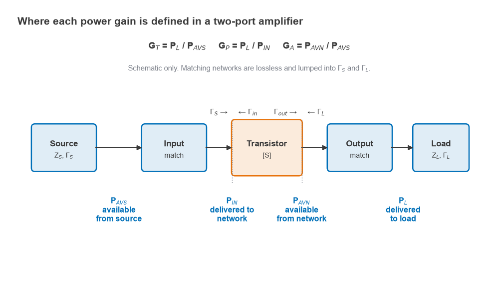
The input and output reflection coefficients of the loaded transistor are needed for all three:
Γin = S11 + S12S21ΓL/(1 − S22ΓL)
Γout = S22 + S12S21ΓS/(1 − S11ΓS)
Γin depends on the load and Γout depends on the source whenever S12 is not zero. That coupling through reverse transmission is what makes bilateral amplifier design harder than simply matching each port separately.
Transducer power gain GT
Transducer gain is the quantity to use when predicting what an amplifier delivers in a system. In terms of S-parameters it is
GT = [(1 − |ΓS|2) / |1 − ΓinΓS|2] · |S21|2 · [(1 − |ΓL|2) / |1 − S22ΓL|2]
The three factors are often read as an input mismatch term, the intrinsic transistor gain and an output mismatch term. An equivalent form that uses only S-parameters and both terminations is
GT = |S21|2(1 − |ΓS|2)(1 − |ΓL|2) / |(1 − S11ΓS)(1 − S22ΓL) − S12S21ΓSΓL|2
When both terminations equal Z0, ΓS = ΓL = 0 and GT reduces to |S21|2. That is why the S21 trace on a vector network analyzer is the transducer gain of the device in a 50 Ω system, and why it is usually well below the gain the same transistor can deliver once matched.
Operating gain GP and available gain GA
Operating gain depends only on the load:
GP = |S21|2(1 − |ΓL|2) / [(1 − |Γin|2)|1 − S22ΓL|2]
Available gain depends only on the source:
GA = |S21|2(1 − |ΓS|2) / [|1 − S11ΓS|2(1 − |Γout|2)]
Each one removes a single termination from the problem, which is useful in design. Power amplifier work usually starts from the load, so constant-GP circles on the ΓL plane are the natural tool. Low-noise design fixes the source for minimum noise, so constant-GA circles on the ΓS plane are plotted alongside noise circles, as in LNA design. Once one termination is chosen, the other is set to the conjugate of the resulting Γin or Γout, and GT then equals GP or GA respectively.
Maximum available gain and maximum stable gain
If the transistor is unconditionally stable, both ports can be conjugately matched at the same time: ΓS = Γin* and ΓL = Γout*. GT, GP and GA are then equal, and their common value is the maximum available gain:
MAG = GT,max = |S21/S12| · (K − √(K2 − 1))
Here K is the Rollett stability factor, K = (1 − |S11|2 − |S22|2 + |Δ|2)/(2|S12S21|) with Δ = S11S22 − S12S21, described fully on the amplifier stability and K-factor page. MAG exists only for K ≥ 1. The required source and load reflection coefficients are
ΓSM = [B1 − √(B12 − 4|C1|2)] / (2C1), B1 = 1 + |S11|2 − |S22|2 − |Δ|2, C1 = S11 − ΔS22*
with the same form for ΓLM after swapping the indices 1 and 2. The minus sign applies when B is positive.
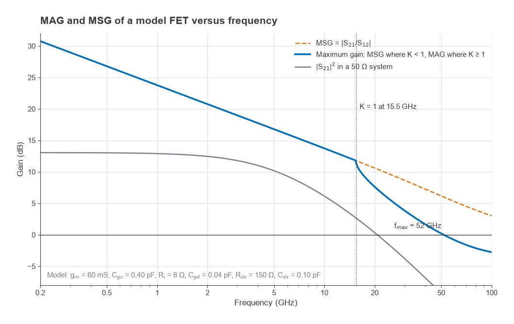
When K < 1 a simultaneous conjugate match does not exist, because the required terminations would make the device oscillate. The figure of merit used instead is the maximum stable gain, MSG = |S21/S12|. It is the value MAG approaches as K falls to 1, and it represents the gain obtainable once the device has been stabilized by just enough added loss to bring K up to 1. Datasheets often plot a single “maximum gain” curve that is MSG at low frequencies, where most transistors are potentially unstable, and MAG above the frequency where K crosses 1.
Figure 3 shows this for a simple FET equivalent circuit (gm = 60 mS, Cgs = 0.40 pF, Cgd = 0.04 pF, Ri = 8 Ω, Rds = 150 Ω, Cds = 0.10 pF). MSG falls at 10 dB per decade, from 20.8 dB at 2 GHz to 13.7 dB at 10 GHz. K reaches 1 at about 15.5 GHz, where the curve switches to MAG and falls more steeply, reaching 0 dB at fmax ≈ 52 GHz. The 50 Ω |S21|2 is only 12.5 dB at 2 GHz, more than 8 dB below the stable gain the same device offers.
The unilateral approximation
If S12 is set to zero, Γin = S11 and Γout = S22, and the ports can be matched independently. The unilateral transducer gain is
GTU = [(1 − |ΓS|2)/|1 − S11ΓS|2] · |S21|2 · [(1 − |ΓL|2)/|1 − S22ΓL|2]
With ΓS = S11* and ΓL = S22* it reaches its maximum:
GTU,max = |S21|2 / [(1 − |S11|2)(1 − |S22|2)]
Whether the approximation is acceptable is judged with the unilateral figure of merit
U = |S12S21S11S22| / [(1 − |S11|2)(1 − |S22|2)]
The true transducer gain then lies within 1/(1 + U)2 < GT/GTU < 1/(1 − U)2. If that error band is small, a fraction of a dB, the unilateral design is good enough and is much quicker to carry out on a Smith chart.
Worked example at 4 GHz
Take a transistor with the following S-parameters at 4 GHz in a 50 Ω system: S11 = 0.72∠−116°, S21 = 2.60∠76°, S12 = 0.03∠57°, S22 = 0.73∠−54°.
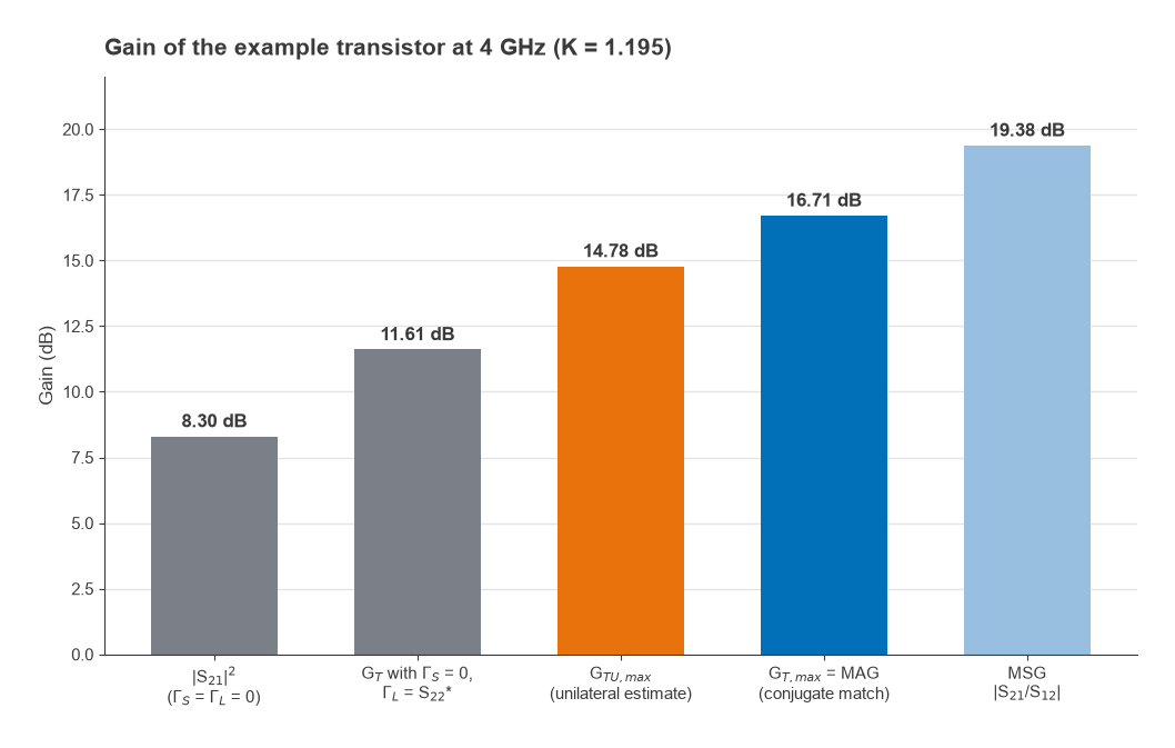
- Stability: Δ = 0.488∠−162.3° and K = 1.195. Both K > 1 and |Δ| < 1, so the device is unconditionally stable and MAG exists.
- Unmatched gain: |S21|2 = 6.76, or 8.30 dB.
- MSG = 2.60/0.03 = 86.7, or 19.38 dB. MAG = 86.7 × (1.195 − √(1.1952 − 1)) = 16.71 dB.
- Simultaneous conjugate match: ΓSM = 0.872∠123.4° and ΓLM = 0.876∠61.0°. Substituting these into the GT formula returns 16.71 dB, confirming MAG.
- Unilateral estimate: the input term 1/(1 − 0.722) adds 3.17 dB and the output term 1/(1 − 0.732) adds 3.31 dB, so GTU,max = 14.78 dB. U = 0.182, giving an error band of −1.45 dB to +1.75 dB. With ΓS = S11* and ΓL = S22* the exact GT is 15.56 dB, inside that band but almost 1.2 dB short of MAG.
A partial design shows how the three gains differ. Leave the source at 50 Ω (ΓS = 0) and set ΓL = S22*. The operating gain is GP = 15.91 dB, but the loaded input reflection is |Γin| = 0.793, a mismatch loss of 10log(1 − 0.7932) = −4.30 dB. GT is therefore 15.91 − 4.30 = 11.61 dB. Because the source is Z0, Γout = S22, the load is its conjugate, and GA is also 11.61 dB. Figure 2 summarizes the results.
Which gain to quote
For system budgets, use GT in the actual source and load environment, since that is what enters a cascade calculation. For comparing transistors or judging how much gain is left at a frequency, use MAG or MSG. For design, pick GP or GA according to which termination is constrained by another goal such as output power or noise figure. Values in dB follow the conventions described in dB and dBm explained, and the matching networks that realize ΓS and ΓL are covered in impedance matching and L-network matching.
Frequently asked questions
What is transducer gain?
Transducer gain is the power delivered to the load divided by the power available from the source. It includes the effect of mismatch at both ports, so it is the gain an amplifier delivers in its real environment. In a matched Z0 system it equals |S21|2.
What is maximum available gain?
Maximum available gain is the transducer gain obtained when both ports of an unconditionally stable transistor are conjugately matched at the same time. It equals |S21/S12|(K − √(K2 − 1)) and is defined only for K ≥ 1. It is the upper limit for a single stage built with lossless matching networks.
What is the difference between MAG and MSG?
MAG applies when K ≥ 1 and is achieved with a simultaneous conjugate match. MSG, |S21/S12|, applies when K < 1 and is the gain available after the device has been stabilized to the K = 1 boundary. At K = 1 the two values are equal.
Why is S21 lower than the gain on a transistor datasheet?
|S21|2 is the gain with 50 Ω on both ports, where a transistor is usually badly mismatched. Datasheet maximum gain curves show MAG or MSG, which assume ideal matching networks. In the 4 GHz example the difference is 8.4 dB.
Related topics
Gain definitions build on S-parameters and lead straight into stability and the K-factor. Measured data for these calculations usually arrives as Touchstone .s2p files. For the broader amplifier picture, see RF amplifiers and broadband RF amplifier design, and for terminology, the wireless terms glossary.