ILLUSTRATION: LUTHER EASON
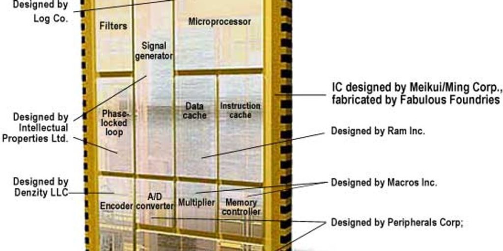
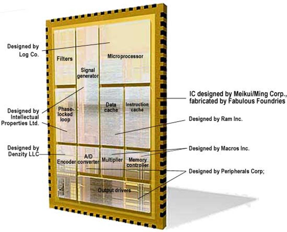
Building a System on Chip: Compatibility is the key to building an SoC, as is illustrated by this fictitious IC design. To build it, a fabless semiconductor company has used blocks of intellectual property (IP) acquired from several IP houses. The fabless designers must ensure all the blocks will work together and be compatible with the semiconductor process of the foundry chosen to fabricate the chips.
The last decade saw a surge in the number of small IC design houses that provide systems manufacturers with application-specific ICs (ASICs). These fabless enterprises, so-called because they farm out IC fabrication to commercial silicon chip foundries, cost relatively little to start up yet can be richly rewarded if the market adopts their products. Sustained by a wealth of design tools, they have earned a place alongside long-established, large chip manufacturers like IBM, Intel, Motorola, and Texas Instruments.
More recently, shrinking circuit features and rising transistor density have spawned the astonishing system on a chip (SoC)[see Fig. 1], in which most or all of the circuitry required for, say, a cellphone fits on a single IC. Today, these SoCs often contain analog, RF, and mixed-signal components to satisfy the growing demands of communication applications.
All the same, the ambitious SoC endeavor risks suffocation by its own success: the number of deployable transistors on a chip far exceeds the design team’s power of arranging them to perform meaningful functions. Evidently, SoC designers need input from the intellectual property (IP) providers that design circuit modules for use with other SoC elements. Also, they need design tools that can rapidly integrate IP libraries with the mundane sizing, placing, and routing of circuits.
In short, electronic design automation (EDA) must do more than keep pace with fabrication technology. It must also come to terms with three disruptive changes already molding its prospects and, by extension, those of the larger IC manufacturing sector. First, there is the growing intricacy of SoC and system-in-a-package applications, especially those with large blocks of analog and RF components. Second, there is the need for fabless semiconductor companies to develop business models for sending IP-based designs to foundries or contract manufacturers.v Third, SoC designers require new integrated hierarchical design flows (running from high-level concepts to netlists and wired gates) that allow IP creation and wide reuse. Taken together, the answers to these needs will mold how SoC and ASIC innovations will be captured and exploited by very large-scale circuitry. And EDA tools are essential to the rapid and inexpensive delivery of semiconductor IP to the IC design house, even for low-volume applications.
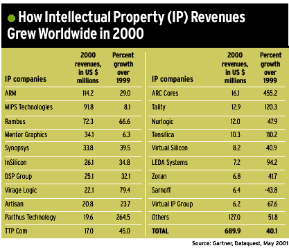
Profits and enormous market growth lie ahead. Commercial IP is one of the most flourishing sectors of the US $800 billion IC market. Consisting of logic, memory, and processor cores developed by third parties for reuse by small design houses and big IC manufacturers, it totaled $690 million in 2000, or 48 percent more than in 1999. The ideal is to enable designers to rapidly plug together an SoC from mix-and-match products made by different IP vendors [see table, below].