IP design opportunities
The IP embodied in synthesized circuits may be divided up into functional blocks for use in different designs and for different applications. The first design groups to realize the benefits of reusable IP were the large IC manufacturers. In the mid-1990s, Intel, ARM, and MIPS Technologies began developing embedded processor cores with instruction sets tailored to the application. Worldwide standardization initiatives such as the System Level Design Language (SLDL), which streamlines IP authoring and SoC integration processes, and VSIA’s Virtual Component Interface standard, which supplies well-defined and open data communication protocols between blocks of IP, encourage this trend.
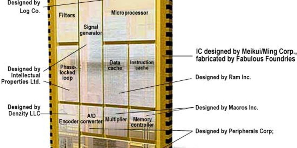
Today, a growing number of IP vendors are offering a wide range of mostly embedded components for digital reuse. Bought off the shelf and integrated into an SoC, these components can make designers an order of magnitude more productive. Moreover, once there is general use of embedded reprogrammable logic to customize an IP block, it will be easier to retarget IP blocks for other specific applications, further enhancing productivity.
Mixed-signal properties
Whereas digital IP processes binary signals, analog IP operates on continuous signals whose voltage is precisely specified. This is an even harder problem for the SoC design houses. For one thing, the hardware description languages used for digital designs contain synthesizing options that cannot be used to create analog blocks. With the arrival in the last few years of VHDL and analog and mixed-signal tools like Varias from Avanti, AMSDesigner from Cadence, and Advance-MS from Mentor Graphics, digital and analog signal responses can be simulated. But the simulation is rudimentary, capable only of switching between the HDL digital description and the Spice-based analog circuit model.
Remember, too, that an analog system is specified by such parameters as gain, noise, slew rate, and common-mode rejection. Accordingly, overall IP performance depends much more on the manufacturing process than does a digital design. For that reason, any reusable analog IP is provided in hard form: it is delivered as a physically laid-out and routed circuit, which is added to the rest of the design.
The combination of reusable analog and digital IP will gain ground generally. IP is already found in 25 percent of today’s SoCs, and that could triple within five years. The analog portion may already absorb more than half the design effort. Especially for fabless companies, retargeting and reusing analog IP will be a prerequisite for success. Recognizing this trend, TSMC as the world’s largest pure-play foundry has already shipped process data of its 0.18-µm CMOS technology to a few providers of analog EDA synthesis tools. Such process information is crucial if analog libraries are to be linkable to the underlying physical deep-submicron technology.
To enhance productivity, third-party vendors of IP will have to offer digital as well as analog and mixed-signal IP as standard libraries, integrated into EDA design flows. As for the tool sets used by design houses, they will have to be flexible enough to manage concurrent hardware-software co-designs. Linear, top-down design flows and the separation of software and hardware design will be things of the past. With the new design flow, designers may use performance as their criterion for partitioning the SoC into hardware and software components and for incorporating digital and analog reusable IP to speed up the design process. The IP will be supplied through standard interfaces, or wrappers, with plug-and-play functionality.
While most engineers view such developments as a distant dream, a small group hails the availability within two or three years of predesigned, preverified, plug-and-play IP cores. They expect the IC design houses could quickly place and route these cores into a standard SoC template for their customers’ applications. After all, they can point to the already posted Design and Reuse IP catalog (www.us.design-reuse. com) of Design-Reuse of Newark, Calif., and Grenoble, France, with more than 1700 cores from 190 companies. While the catalog is not as extensive on the analog side and lacks plug-and-play IP capabilities, it indicates how the IP market will evolve.
Next-generation IC technology with 0.1-µm channel size can lead to a lengthy production process: the masks alone take three months to create, and cost over $800 000 each. Costs go even higher when masks require extra features to accommodate the analog portion of a mixed-signal chip. Then, too, the proliferation of 300-mm wafers will raise economy-of-scale issues, as design houses get better at anticipating customers’ needs and automate manufacture to effectively populate the wafer. Indeed, larger wafers could become a problem for fabless companies that need only small batches of chips to supply a niche market; they may instead have to turn to more generic, application-specific, reconfigurable, and retargetable systems. And these needs will of course require ever more integration and innovation from the design tool vendors.
–Linda Geppert, Editor
About the Authors
PETER LEVIN (M) & REINHOLD LUDWIG (SM) are both associated with Techno Venture Management (TVM), an international private equity investment firm with offices in Munich, Boston, and San Francisco. Levin is a partner in the firm, and Ludwig serves as a technical advisor to the company. Ludwig is also a professor of electrical engineering at Worcester Polytechnic Institute.
To Probe Further
The International Technology Roadmap for Semiconductors (http://public.itrs.net) provides one of the most comprehensive reviews of future developments in the electronic design space.
For information about analog circuit synthesis tools, check out the Web site of Neolinear Corp. , Pittsburgh (www.neolinear.com), one of the leaders in analog, mixed-signal, and RF designs.
A host of useful white papers on the current state of electronic design can be found on Cadence’s Web page (http://www.cadence.com).
For a detailed look at how a complex system on a chip (SoC) is created, refer to “A mixed-signal 0.18-µm CMOS SoC for DVD systems with 432-MSample/s PRML read channel and 16-Mb embedded DRAM,” a DVD system on a chip described by T. Yamamoto and his colleagues in the IEEE Journal of Solid State Circuits, Vol. 36, No. 11, pp. 17851793, November 2001.
