The world of analog (low- and, increasingly, high-frequency) circuits is less structured than the digital–hence the paradigm shift presently reshaping the EDA industry. Whereas design flow has centered on the ever-increasing performance of digital components, the revised methodology must systematically embrace both digital and analog components and also take full advantage of reusable IP.
A case in point involves two companies from San Jose, Calif.: inSilicon Corp., a provider of wired and wireless IP communication circuits, and SoC developer Palmchip Corp. The pair has teamed up to provide application-specific SoCs. InSilicon’s IP portfolio bulges with more than 700 analog and mixed-signal IP cores. The company’s IP will be used in CoreFrame, Palmchip’s on-chip interconnect architecture whose synthesis-friendly environment facilitates the plug-and-play of IP from many sources.
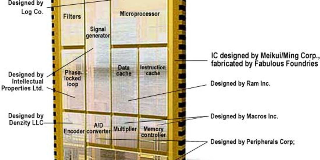
Generically speaking, the design flow of the future identifies filters, amplifiers, and phase-locked loops as blocks, each of which is refined into its constituents–so-called standard macro cells like comparators and inverters–eventually arriving at the physical transistors, resistors, capacitors, and inductors. At each level of refinement, a top-down synthesis is executed followed by a bottom-up layout and verification loop. This process establishes specifications for the next lower level of granularity–the partitioning of a macro into smaller entities, called sub-blocks–and constraints on each block to be passed on to the next level [see figure].
Key design flow details must change, too. At present, for instance, synthesis tools incorporate statistical models of wire-loads that assign lumped-circuit parameters such as capacitance and resistance to the interconnects; this accounts for parasitics and load-dependent timing constraints. But the migration to deep-submicron technology and smaller gate widths demands full-wave solutions instead.
Mix-and-match intellectual property
The capital needed to underwrite a complex SoC design and fabrication process is prohibitive, and only the largest IC manufacturers can afford to operate their own foundries. Soon, with new plants approaching $2.5 billion apiece, owning a dedicated facility will become even harder for many chipmakers to justify. These fixed costs have led almost by themselves to the emergence of dedicated foundry services, whose sole business is custom (and high-volume) IC manufacturing. The first commodity foundries like UMC and TSMC appeared in the early and mid-1980s. These pure-play foundries build 12 percent of all ICs today, and are predicted to reach 26 percent by 2004.
Accordingly, small, mid-size, and even large companies like Motorola, LSI Logic, Chip Express, and Samsung are relying less on in-house foundries. Instead, they offer customers their expertise in planning, design, assembling, and testing and leave the burden of IC manufacturing to dedicated, pure-play foundries such as TSMC, Chartered, UMC, and Siterra. In fact, Motorola’s Semiconductor Products Sector plans to outsource half its off-the-shelf chip production by the end of 2002. Yet as recently as 1998, less than 6 percent of its chips were manufactured outside.
These fabless businesses have compelling advantages. Without huge fixed foundry costs, even low SoC production volume turns a profit. Design methods can be adopted from those EDA suppliers that offer the best single-purpose, or point, solutions. And as a third party slotted between customer and foundry, the fabless business has no conflict of interest; IP can be procured and fabricated to best solve the technical objectives.
On the downside, fabless SoC design houses could lack for foundry capacity. While not an issue at present, with total foundry utilization at an all-time low of less than 40 percent, it may become one. One remedy is to form strategic alliances with foundries, and even acquire partial ownership of them, so as to ensure a say in capacity allocation. Nonetheless, designing SoCs through third-party EDA tools, purchasing or licensing IP, and outsourcing the IC manufacturing requires a cohesive, highly complex business model.
