An overview of the INSPIRE project, connecting building-block innovation to high-growth markets.
(Credit: AMIRES)
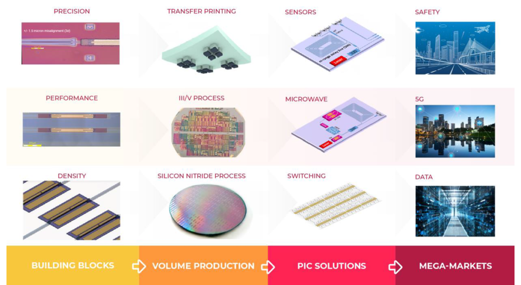
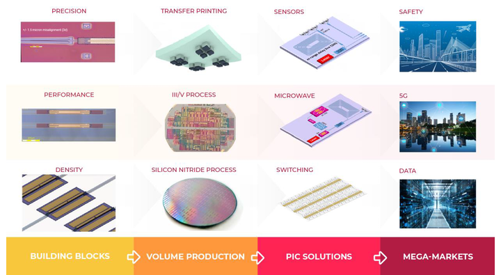
A Horizon 2020 project called INSPIRE will revolutionize photonic integrated circuit (PIC) technology by combining the highest optoelectronic efficiencies in indium phosphide (InP) photonics and lowest optical loss in silicon nitride (SiN) photonics, in a single platform through wafer-scale microtransfer printing technology.
Major photonic integration platforms (SiN- or InP-based) are now mature and making their impact in the real world by, for example, enabling the Internet. The potential for wider impact in other fields, such as sensors, is clear. However, the performance tradeoffs within a single platform are sometimes limiting the uptake. Most notably are applications in high-performance fiber sensors used in infrastructure monitoring and microwave signal processing for radar systems, which would require low-noise operation, the combination of best-in-class active mediums such as lasers, modulators, and photodetectors, and ultra-low loss waveguide propagation. By ensuring scalability and manufacturability, major impact on these demanding application fields is expected.
The INSPIRE project platform, through wafer-scale microtransfer printing technology, will enable a combination of high-performance III-V optoelectronic components, such as InP-based semiconductor optical amplifiers, high-speed modulators and photodetectors, operating in the C-band, with the low-loss passive functionalities of the SiN platform, like filters and delay lines. The microtransfer printing integration, on 200 mm silicon wafers, enables high-throughput integration of III-V devices on SiN PICs, which is key for low cost and scalability. To show the potential to impact a wide range of high-volume-markets, the INSPIRE technology will be validated by three use cases: a distributed fiber-sensing readout unit, a microwave photonic radio-frequency pulse generator, and a datacenter switch fabric. Compact models of the III-V optoelectronic components will be developed, enabling designers to exploit this platform for a wide range of applications.
INSPIRE will sustain Europe’s industrial leadership in photonics by combining the generic integrated foundry technology at the pioneering pure-play foundry SMART Photonics (Eindhoven, Netherlands) and silicon photonics pioneer imec (Leuven, Belgium), with the microtransfer printing technology at X-Celeprint (Cork, Ireland), making this a platform that combines the strengths of two of the most well-known PIC manufacturing platforms. It will also strengthen the European manufacturing base by developing and implementing processing steps that are key to removing expensive assembly steps in PIC-based product realization. The methods will be developed for SiN-InP integration, but can be transferred to silicon photonics as well.
INSPIRE creates a full-function PIC platform, compatible with open-access pilot manufacturing and with an order-of-magnitude lower cost for volume production. The generic approach makes the technology widely applicable and ensures that European innovators can focus their research and development directly on manufacturing platforms for shorter time to market.
The INSPIRE project began January 1, 2021, with an expected duration through June 30, 2024.
