
Illustration: Bryan Christie Design
Remember when combining a camera with a cellphone seemed daring? Or adding a cellphone to a PDA? Such technical tricks relied on Moore’s Law, which holds that the number of transistors on an IC doubles every 18 months. In the computing world, having more transistors on a chip means more speed and possibly more functions.But in many cases, those Moore’s Law ICs deal with only 10 percent of the system. The other 90 percent is still there, showing up as an array of bulky discrete passive components—such as resistors, capacitors, inductors, antennas, filters, and switches—interconnected over a printed-circuit board or two. Real miniaturization requires something more, and we have it in the system-on-package (SOP) approach we’re pursuing at the Microsystems Packaging Research Center at the Georgia Institute of Technology, in Atlanta. SOP leapfrogs well beyond Moore’s Law. It combines ICs with micrometer-scale thin-film versions of discrete components, and it embeds everything in a new type of package so small that eventually handhelds will become anythingfrom multi- to megafunction devices. SOP products will be developed not just for wireless communications, computing, and entertainment. Outfitted with sensors, SOPs could be used to detect all manner of substances, toxic and benign, including chemicals in the environment, in food, and in the human body.
This last application will see the convergence of biology, chemistry, and digital technology to produce capsules small enough to be introduced into the human body to monitor personal health daily. A capsule could be used, for example, to check vital signs and monitor parameters such as glucose levels, blood pressure, and even signs of cancer. The capsule would then wirelessly communicate the person’s health status to a Web terminal outside the body or, via the Internet, to a physician (or to anyone, anywhere). Fitted with a reservoir, the capsule could also deliver drugs at programmed intervals to selected places within the body.
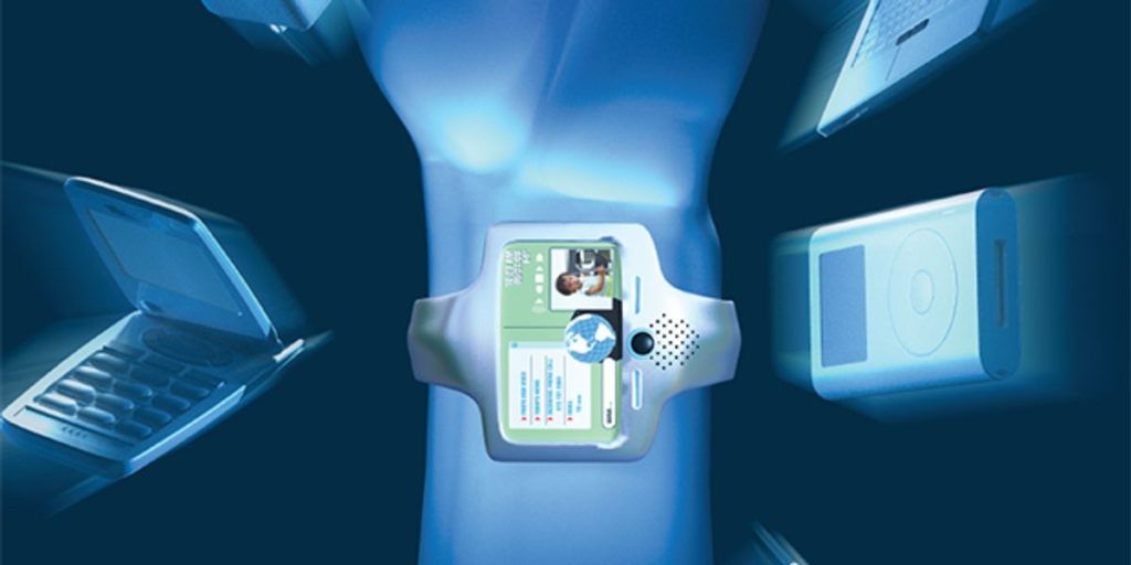
That tiny body capsule is certainly a compelling product, and we can expect many others. Imagine, for example, a home entertainment and control hub—a device that combines voice, video, data, sensing, and control functions. It could include a home computer, a cellphone, environmental and other sensors, a health monitoring device, and a satellite TV receiver, to name just some possibilities. A wireless broadband connection would link the system to the Internet, and the hub would serve as the remote control for all the home’s appliances.
Yet the hub would be as small as a credit card.
We envision a megafunction SOP unit built with microscale components that would be the size of an Intel Pentium processor, which comes in a flat pack 35 centimeters on a side. Or, built with nanoscale technologies, an SOP could be as small as a millimeter on a side. SOP products will attain such small sizes because the technology attacks the 90 percent of the system—the so-called 90 percent problem—that is not integrated [see diagram, “Many in One”].
In a cellphone, for example, that 90 percent typically adds up to some 400 discrete passive components and their metal interconnections, all fastened to a relatively large printed-circuit board. And, of course, some systems will have thousands of discrete components sitting on circuit boards.
SOP technology represents a radically different approach to systems. It shrinks bulky circuit boards with their many components and makes them nearly disappear. In effect, SOP sets up a new law for system integration. It holds that as the components shrink and the boards all but disappear, the component density will double every year or so, and the number of system functions in an SOP package will increase in the same proportion. Thus, SOP technology yields far more in system miniaturization than can be expected from Moore’s Law, which deals only with transistors in ICs [see graph below, “Growing Faster”].
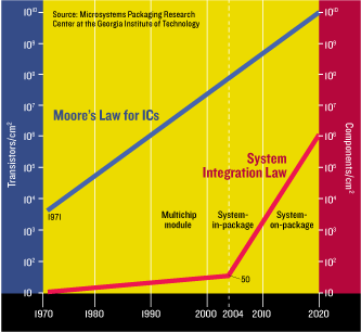
Growing Faster: System integration using system-on-package (SOP) technology from Georgia Tech’s Microsystems Packaging Research Center will see “More Than Moore’s Law” take hold, as measured by component density. From about 50 components per square centimeter in 2004, component density will climb to about a million per square centimeter by 2020. Functional system density will escalate similarly.
Squeezing so much into tiny spaces is our mission at Georgia Tech. If we have our way, products will shrink by much more than the factor of 10 typically expected every few years now. Instead, they will shrink by factors of many hundreds and even thousands in the same time frame.
We began this research in 1993 with a proposal to the U.S. National Science Foundation for an Engineering Research Center, which the NSF then funded. Today we are not alone in this endeavor: researchers around the world are using SOP to combine diverse technologies in new, unusual, and cost-effective ways. Everyone is after ultracompact products built with any combination of digital, analog, radio-frequency, and even optical circuitry, as well as a variety of sensors.
