For more than 40 years, circuit designers have counted on the steady increase in transistor density in their pursuit of convergence. For example, engineers at Texas Instruments are building entire signal-processing subsystems with diverse functions on a chip of silicon—a system-on-chip, or SOC, as it’s called. Designing such a chip has its technical problems, too, particularly if digital logic and memory for computation must be combined with analog and RF communications circuitry. Usually, these dissimilar circuits not only operate at different voltages but also require different processing steps during manufacture. Complicating matters further, analog and RF circuits must be electrically isolated from digital ones. Design time and complexity, along with fabrication costs and time to market, can skyrocket.
At Georgia Tech we take advantage of package integration. We eliminate the individual passive component packages—the hard black tiles you see on the large system board inside your PC, DVD player, or cellphone. Those packages measure anywhere from a quarter of a millimeter to as large as 3 cm on a side and a millimeter or two high. Instead of using them, we convert the passive elements to bare, thin-film components only micrometers thick and embed them in our multilayered system package. Such thin-film components are anywhere from a thousandth to a millionth of their original packaged size. Further, in our latest research, we have eliminated bulky IC packages, too, by embedding their bare chips in the SOP package. We even shave the chips down to a thickness of 25 micrometers, from their original 1 millimeter.
SOP does away with the bulky system board and makes the package the centerpiece of system integration. Highly integrated, this multilayered package holds all the parts—thinned, bare IC chips; passive thin-film components; and wiring and interconnections.
The result is that we raise the component count—and the number of functions—per unit volume well beyond what is possible by ignoring the package and simply relying on Moore’s Law for ICs. But smaller size is not the only benefit. Size reduction also allows for much faster chip-to-chip signals at lower currents and voltages—which cuts power dissipation.
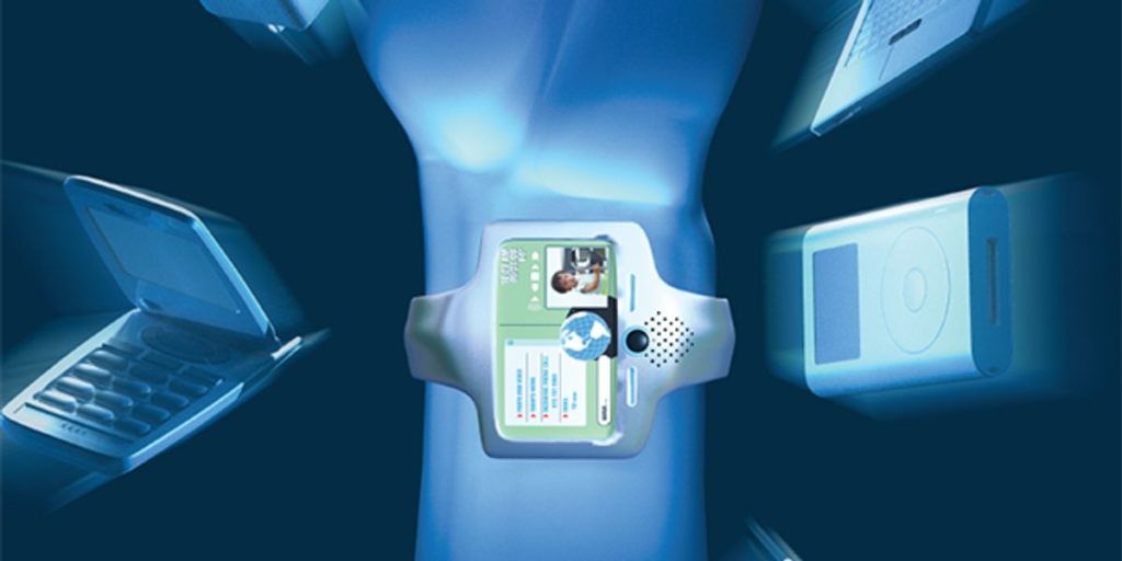
ICs and discrete components are combined in such a small package that, eventually, handhelds will become megafunction devices
Note, too, that with SOP we’re not limited to silicon or any particular technology; we can use whatever we wish. Another benefit is that we don’t force dissimilar technologies to cohabit on a single piece of silicon, as may happen in an SOC design that tries to put many functions on a single IC chip.
We use devices made of silicon, gallium arsenide, or silicon germanium—whatever material is best suited for our ICs and discrete components [again, see “ ”]. For example, we use silicon ICs for digital circuits and some RF devices, such as amplifiers and oscillators. In the package, we embed antennas, capacitors, inductors, resistors, filters, crystals, and waveguides. We embed these parts as thin films in the layers of the package. For biosensing applications, we form sensors of tiny resonators, nanotubes, nanobelts, and microelectromechanical systems (MEMS). And when quantum and molecular devices become available, we’ll be able to use them, too.
Because we’re not forced to use any particular technology, the time it takes to design and fabricate a system is much shorter than before, and time to market is shorter as well. Further, the circuitry and package of an SOP-based system are designed and fabricated in parallel—not serially, one after another—which saves time and money.
We need not compromise speed, cost, time to market, or reliability. Such compromises must be made when dissimilar technologies are combined in a single IC. Yet our SOP with its many functions will be no bigger than the bulky package of an SOC, which cannot combine nearly as many technologies as we can. Our SOP can even provide cost-effective chip-to-chip optoelectronics, replacing copper wire with optical fiber, and can include miniature waveguides, gratings, lasers, and detectors.
To build an SOP for, say, a mixed-signal, multifunction system, we can fabricate multiple system functions on a single substrate. We start with an ultrathin yet stiff composite substrate. Next we deposit layers of dielectrics and conductors as well as the thin-film components, including capacitors, resistors, inductors, filters, switches, and waveguides. But unlike a silicon wafer, which is round, our SOP wafer is square, measuring, so far, 300 mm on a side. Completed wafers are electrically tested and diced into square or rectangular system packages measuring anywhere from 1 to 2.5 cm on a side. Some ICs of silicon or gallium arsenide or other material—whether meant for processors or memory—can be connected to the top surface of the SOP with ordinary lead-free solder or copper interconnects.
Our SOP concept goes well beyond merely placing multiple chips in a package, as IBM did some 20 years ago in its ceramic multichip module. Until our SOP came along, IBM’s MCM was the most highly integrated package in existence, with copper wiring for interconnecting ICs. But it has no embedded thin-film components as does an SOP, and it requires a system board. Thus, while an SOP attacks the 90 percent part of the system problem, an MCM does not.
SOP is also different from a system-in-package (SIP), another miniaturization technique being deployed by most IC, package, and cellphone companies. In the SIP approach, bare or packaged IC chips are stacked on top of each other in a three-dimensional arrangement. But SIPs address only 10 percent of the system problem and ignore the problem of bulky passive components. An MCM or an SIP must still plug into a traditional system board.
