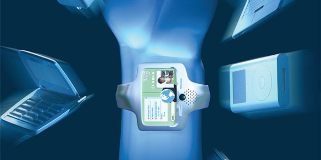
Our SOP has many advantages over those other approaches. Perhaps the biggest benefits are that, in a cellphone, for example, we have none of those 400 passive components to assemble, and there is no system board, since the board becomes the package. And the package can hold silicon digital ICs alongside ICs made of other materials. Such capability is next to impossible for an SOC and has not been demonstrated for an SIP.
Because an SOP uses separate chips for its different functions, designs are simpler and manufacturing time shorter than for an SOC. And for computing applications we can even remove the space-eating and high-resistance wires on the ICs that distribute clock and power. Instead, we put those wires in our package. We can also move nanoscale wiring that is on chip into the package. There, such wires can be wider and thicker than what can be reasonably fabricated on chip; wire resistance is lower, improving speed and reducing the energy lost to heat.
An SOP design relies on many thin horizontal layers of dielectrics holding conductors and components. For computing applications, we deposit multiple layers of ultra-low-loss and ultra-low-dielectric-constant insulators along with electroplated copper interconnects made of 2- to 5-mm-wide copper traces. The insulators are made of conventional polymers, such as epoxies, or more advanced polymers, such as polyimide or benzocyclobutene, that have outstanding dielectric properties.
We also embed 1-µm-thick decoupling capacitors very close to each IC chip to minimize power noise. To accomplish this, we invented novel ceramic decoupling capacitors that can be processed at relatively low temperatures. Traditionally, ceramics have the highest dielectric constant and lowest dielectric loss, compared, for example, with organic materials. Ceramics’ drawback is that the capacitors must be fabricated at very high temperatures, well beyond what is typical of electronics fabrication. Capacitors made of organic materials, on the other hand, can be fabricated at lower temperatures but suffer from very low dielectric constants. We developed capacitors with ceramiclike properties but fabricated at the temperatures used for organic materials in an advanced low-temperature chemical process referred to as a hydrothermal process.
For RF applications, we form organic-compatible thin-film capacitors that are stable because of their low temperature coefficient of capacitance. We also fabricate high-value resistors that are stable because they have a low temperature coefficient of resistance. We form high-quality-factor inductors far superior to any fabricated on silicon. We use a variety of both thin-film and composite technologies to achieve these properties. Thin-film fabrication processes include sputtering, electroplating, and sol gel, as well as the hydrothermal process.
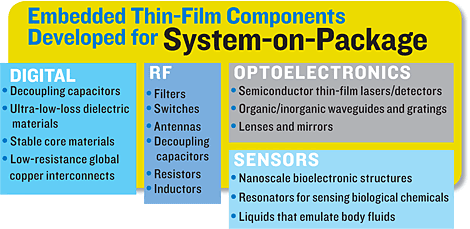
For optical applications, we deposit thin films to form waveguides, optical gratings, mirrors, and lenses. For sensing biological functions in the body, we have developed silicon, zinc oxide, and carbon nanotube sensors that selectively detect the chemicals of body fluids. [See chart, “Embedded Thin-Film Components Developed for System-on-Package.”]
We have also built numerous research vehicles that combine RF, digital, and optical functions. The Intelligent Network Communicator was the first such mixed-signal SOP, designed and built at the Microsystems Packaging Research Center in 2003. We used it to learn how to simultaneously design, develop, and optimize our materials and processes. It was a 75- by 50-mm multilayer sandwich, 1.2 mm thick, made of thin-film materials and embedded active and passive components and active devices in packages on the top surface.
We built it to transmit a high-speed digital signal on an RF carrier over an optical channel to help us understand the design and interface issues inherent in combining these technologies. The unit consists of a field-programmable-gate-array (FPGA) IC for the transmitter and another for the receiver.
Each IC supports 16 channels, each with a speed of 155 megabits per second. The transmitter output is multiplexed to generate a 2.4-gigabit-per-second digital data rate that modulates a 5.8â’’gigahertz RF carrier. The modulated signal is transferred to the optical circuitry, which consists of a bare laser diode, waveguide, and photodetector.
The laser diode converts the signals, which are then transmitted as light through the waveguide to the photodetector. Converted at the photodetector, electrical signals return to the analog section, where they are converted back into a digital data stream and received by the FPGA. In the digital section the data are compared with the original transmitted data. The streams should be identical.
The measured waveforms on the module surpassed the design goals, indicating the robustness of our process. For example, the digital block was designed for a 2.4-Gb/s digital data rate, but we found we could send a data stream at up to 3.1 Gb/s. Similarly, the optical waveguide supported a 10-Gb/s data rate with minimal degradation.
The eight thin-film layers of the communicator system board include four dielectric layers holding copper interconnects. Wiring patterns are produced on different layers with advanced photolithographic printed-wiring techniques. Microvias connect the buried wires to digital and RF circuitry both within the package and to ICs on the surface. Thin-film capacitors deposited on one of the board’s wiring layers act as decoupling capacitors to suppress power noise. With our techniques, we routinely achieved densities of 400 components per square centimeter, a figure recently improved to 600–1000/cm2. We expect to reach 10 000/cm2 within a decade. Until recently, the component density of electronic systems on conventional circuit boards stood at about 50–100/cm2.
Since we began developing the SOP concept in 1993, we have worked with more than 100 electronics companies from the United States, Japan, Korea, and Europe. Included are Advanced Micro Devices, Asahi, Ericsson, Ford, Hitachi, IBM, Intel, Matsushita, Motorola, NEC, Nokia, Samsung, Sony, and Texas Instruments. In addition, more than 70 researchers have come as visiting engineers to our center to study SOP and its application to their diverse requirements.
So far, at least 50 companies have taken parts of our technology and applied them to their automotive, computer, consumer, military, and wireless applications. We have also built a number of test vehicles for different companies focused on integrating different combinations of analog, digital, RF, optical, and sensor components in a single package.
Motorola, for example, which was one of the Packaging Research Center’s founding partners, uses parts of SOP technology in two models of its GSM/General Packet Radio Service quad-band cellphones to gain about a 40 percent reduction in board area. The module contains all the critical cellphone functions: RF processing, base-band signal processing, power management, and audio and memory sections. Not only does the module free up space for new features, it is also the base around which new cellphones with different shapes and features (camera or Bluetooth, for instance) can be rapidly designed. Motorola calls its package a system-on-module (SOM), for which it developed its own custom embedded-capacitor technology. It reports it has shipped more than 20 million SOM-based phones.
SOP research is flourishing around the world. At the Institute of Microelectronics in Singapore, for example, Mahadevan Iyer and his co-workers have built an optoelectronic SOP intended for high-speed communications between a network and a home or office. The approach is slightly different from ours, with optical circuits made of silicon. The system transmitted data at 1 GHz. Someday such a device might operate at hundreds of gigabits per second.
At the Interuniversity Microelectronics Center, in Leuven, Belgium, Robert Mertens and colleagues are studying the best type of RF antenna to build in an SOP for a range of wireless communications products yet to be introduced.
At the University of Arkansas, in Fayetteville, Len Schaper and Richard K. Ulrich developed techniques for burying capacitors, resistors, and inductors in the layers of their SOP board. They determined that almost all the resistance and much of the capacitance needed for a system can be embedded in the board using vacuum-deposition processes typical of the IC industry.
At the Royal Institute of Technology, in Stockholm, Sweden, Hannu Tenhunen and his group are comparing the cost of an SOP to the cost of an SOC-based system to better understand SOP’s cost advantages. And at Georgia Tech we have applied innovative and low-cost chemical processes to form more than 20 thin-film digital, RF, optical, and sensor components for SOPs. Included are embedded capacitors in the microfarad range, up from the nanofarad, where they had been.
The next step for SOP is to add optical signaling between chips inside the package by sending light signals through built-in optical waveguides. This way, a microprocessor will be able to exchange data with a memory chip at processor clock rates, rather than at the few hundred megahertz possible now.
The main problem with optoelectronics has not been performance but high cost. However, we can reduce cost by building SOPs in batches. For example, as is done for ICs, hundreds of small optoelectronic SOPs could be fabricated on a single large board of 400 by 500 mm. Individual packages measuring, say, 25 mm on a side could then be cut from the board much as individual dies are cut from a large silicon wafer.
In addition to waveguides, we have built complete thin-film, chip-to-chip optoelectronic systems that include lasers, optical gratings for selecting specific wavelengths, microlenses for focusing light onto gratings, and photodetectors. Most of the structures have been made with light-sensitive polymers and lithographic techniques similar to those used to make ICs.
