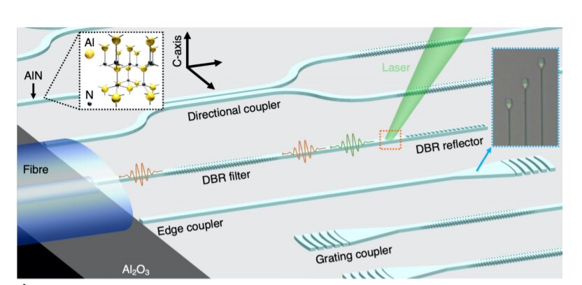
. Blue inset: Microscope image of the fabricated QE-integrated waveguides, where the grating couplers are used for visual feedback during fibre edge coupling. Credit: ACS Photonics")
Quantum emitters are key for a range of technologies including LEDs, lasers and, in particular, photonic quantum communication and computation protocols. So far, scientists have turned to diamond and silicon carbide (SiC) to develop single photon sources on account of their wide band gap and excellent optical properties. However, the shortcomings of these semiconductors are highlighted by attempts to manipulate and route this kind of quantum emission in an integrated fashion to create scalable systems.
Now Tsung-Ju Lu and Benjamin Lienhard, and a team of researchers at the Massachusetts Institute of Technology (MIT) and City University of New York in the U.S., led by MIT’s Dirk Englund, have produced quantum emitters in a III-V semiconductor, aluminum nitride (AlN). AIN is already well established in the optoelectronics and high-voltage electronics industry. By patterning the AlN with the quantum emitters embedded, they were able to integrate the emitters directly into a photonic circuit.
Getting quantum emission
Lu describes quantum emitters as light sources that emit single photons. “They can potentially have electron spin states that can form a quantum bit, or qubit, in which the single particles of light emitted by the quantum emitter carry the qubit’s information,” he tells Phys.org. It’s in routing the qubit’s information using photonic integrated circuits that problems arise with quantum emitters produced in diamond or SiC, because researchers can’t grow these materials as thin films on a low refractive index substrate, which is needed for the total internal reflection in photonic waveguides.
One promising way around this is to combine these materials with other materials already well established as photonic integrated circuit platforms to re-route the photons produced, but this introduces potential inefficiencies when connecting between different materials. Lu and his colleagues had already developed an AlN-on-sapphire photonics platform for the purpose of interfacing with well-studied quantum emitters in other materials like diamond.
“As AlN has one of the widest bandgaps among all semiconductor materials, it was natural for us to explore whether or not AlN itself can be host to quantum emitters that can be readily integrated and connected to our AlN-on-sapphire photonics platform,” he says.
Heated to perfection
The researchers started with wafers composed of densely packed hexagonal nanocolumns of AlN grown on top of sapphire and produced quantum emitters in the material by bombarding it with helium ions using a helium ion microscope to produce vacancy-based defects in which one atom in the crystal lattice is missing. The defect centers have an electronic energy level structure akin to that of atoms. As such, the defect center can be stimulated to the excited state by shining a laser on it, and a single photon is emitted when it decays back to the ground state. This single photon emission has an “anti-bunching” characteristic—because the quantum emitter emits only one photon at a time, a finite period of time passes between photon emissions.
Semiconductors typically require high crystallinity in order to host stable quantum emitters. The catch is that when AlN films grow on some other material, for example, sapphire as in the current work, it needs to be quite thick to establish high crystallinity. As a result, when the researchers studied their thin films treated with helium ions followed by annealing at 700 degrees C to form quantum emitters, their photoluminescence measurements were swamped with background noise, hiding the presence of quantum emitters. Fortunately, they found that high-temperature treatment at an even higher temperature of 1000 degrees C could improve the crystallinity to a sufficient degree to resolve single photon emitters.
The researchers measured and characterized the quantum emitters in samples annealed at 1000 degree C, which were shown to have a high emission count rate while maintaining exceptional single-photon purity, all while operating at room temperature. Furthermore, by patterning the sample with elements such as distributed Bragg reflectors, spectral filters, beam splitters and edge or grating couplers, they could directly integrate the quantum emitters into photonic circuits, showing the potential for creating high-quality quantum emitters monolithically integrated in a wide range of AlN-based devices.
Having established the excellent optical properties of the AlN quantum emitters, the researchers next intend to pinpoint their exact origin to gain an insight into whether they have spin states that can be optically controlled to act as qubits.
Tsung-Ju Lu et al. Bright High-Purity Quantum Emitters in Aluminum Nitride Integrated Photonics, ACS Photonics (2020). DOI: 10.1021/acsphotonics.0c01259
© 2020 Science X Network
Citation:
III-V semiconductor photonic integrated circuits go quantum (2020, October 5)
retrieved 5 February 2021
from https://phys.org/news/2020-10-iii-v-semiconductor-photonic-circuits-quantum.html
This document is subject to copyright. Apart from any fair dealing for the purpose of private study or research, no
part may be reproduced without the written permission. The content is provided for information purposes only.
