
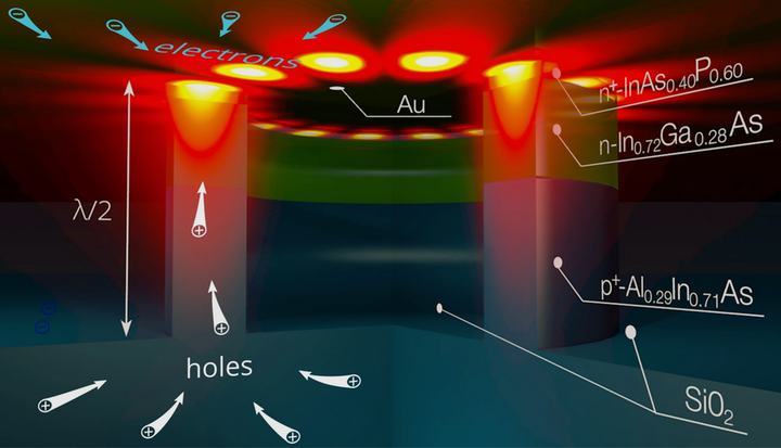
An electrically pumped ring-shaped surface plasmon-polariton nanolaser double heterostructure consists of an InAsP/InGaAs/AlInAs layer stack on AlInAs surrounded by silicon oxide and a gold superstrate.
(Image credit: Dmitry Fedyanin)
Of all the components in a photonic integrated circuit, the laser light source is the most problematic; because silicon itself does not easily emit light, other semiconductors more suitable as light emitters must typically be fabricated on silicon to create a hybrid structure. A new entry of this type has been created by researchers from the Moscow Institute of Physics and Technology (MIPT) and King’s College London, who have cleared the obstacle that had prevented the creation of electrically driven nanolasers for integrated circuits.1 The approach, based on a double-heterostructure tunneling Schottky barrier diode, could help lay the foundation for ultrafast optical data transfer in the many-core computer microprocessors expected to emerge in the near future.
Creating a 1000-core processor that would be on the order of 100X faster than its 10-core counterpart is being pursued by semiconductor industry giants IBM, HP, Intel, Oracle, and others. Such an achievement would make it possible to design a true supercomputer on a single chip. The challenge is to connect optics and electronics at the nanoscale. To achieve this, the optical components cannot be larger than hundreds of nanometers. This size restriction also applies to on-chip lasers, which are necessary for converting information from electrical signals to optical pulses that carry the bits of the data.
Replacing photons with surface plasmon-polaritons
However, the quantum uncertainty principle says there is a minimum volume that photons can be localized in: such a volume cannot be smaller than the cube of the photons’ wavelength. That said, there is a way around this restriction on the size of optical devices: photons can be replaced with surface plasmon-polaritons (SPPs).
Only a few metals, known as plasmonic metals, are good to work with SPPs: gold, silver, copper, and aluminum. SPPs are electromagnetic waves, but at the same frequency they are much better localized than photons. Using SPPs instead of photons makes it possible to “compress” light and thus overcome the diffraction limit.
The design of truly nanoscale plasmonic lasers is already possible with current technologies. However, these nanolasers are optically pumped, making them unsuitable for use on electronic chips. A chip intended for mass production and real-life applications must incorporate hundreds of nanolasers and operate on an ordinary printed circuit board. A practical laser needs to be both electrically pumped and operable at room temperature (the latter of which negates the use of the titanium or chromium required for the ohmic contacts in such lasers).
The new scheme for electrical pumping, confirmed as of now by computer modeling, is based on a silver (Au)/indium arsenide phosphide(InASP)/indium gallium arsenide(InGaAs)/aluminum indium arsenide (AlInAs) double heterostructure with a tunneling Schottky contact, which makes the ohmic contact, with its strongly absorbing metal, redundant. The pumping now happens across the interface between the plasmonic metal and semiconductor, along which SPPs propagate. “Our novel pumping approach makes it possible to bring the electrically driven laser to the nanoscale, while retaining its ability to operate at room temperature,” says Dmitry Fedyanin of the Center for Photonics and 2D Materials at MIPT. “At the same time, unlike other electrically pumped nanolasers, the radiation is effectively directed to a photonic or plasmonic waveguide, making the nanolaser fit for integrated circuits.”
Ring resonator
The laser cavity has a subwavelength ring-resonator design with an InGaAs active layer; the laser emits at a 1.95 μm (which is easily transmitted in silicon waveguides). The volume occupied by the SPPs in the proposed nanolaser is 30X smaller than the light wavelength cubed. According to the researchers, their room-temperature plasmonic nanolaser could be easily made even smaller, making its characteristics even more impressive, but that would come at the cost of the inability to effectively extract the radiation into a bus waveguide. Thus, while further miniaturization would render the device poorly applicable to on-chip integrated circuits, it would be still convenient for chemical and biological sensors and near-field optical spectroscopy or optogenetics.
Despite its nanoscale dimensions, the predicted output power of the nanolaser amounts to more than 100 μW, which is comparable to much larger photonic lasers. Such a high output power would allow each nanolaser to be used to transmit hundreds of gigabits per second, say the researchers, eliminating one of the most formidable obstacles to higher-performance microchips.
REFERENCE
1. D. Y. Fedyanin et al., Nanophotonics, 9, 3965–3975 (2020); https://doi.org/10.1515/nanoph-2020-0157.
