Intel unveiled its second-generation quantum computing control chip during its Intel Labs virtual event today. The chip, codenamed Horse Ridge II, is another milestone toward making quantum computing — one of the holy grails of computing — more practical. The new prototype builds on the first-generation Horse Ridge controller introduced in 2019. Horse Ridge II has more capability and higher levels of integration to control a quantum computer, which remains a long-term goal for the company.
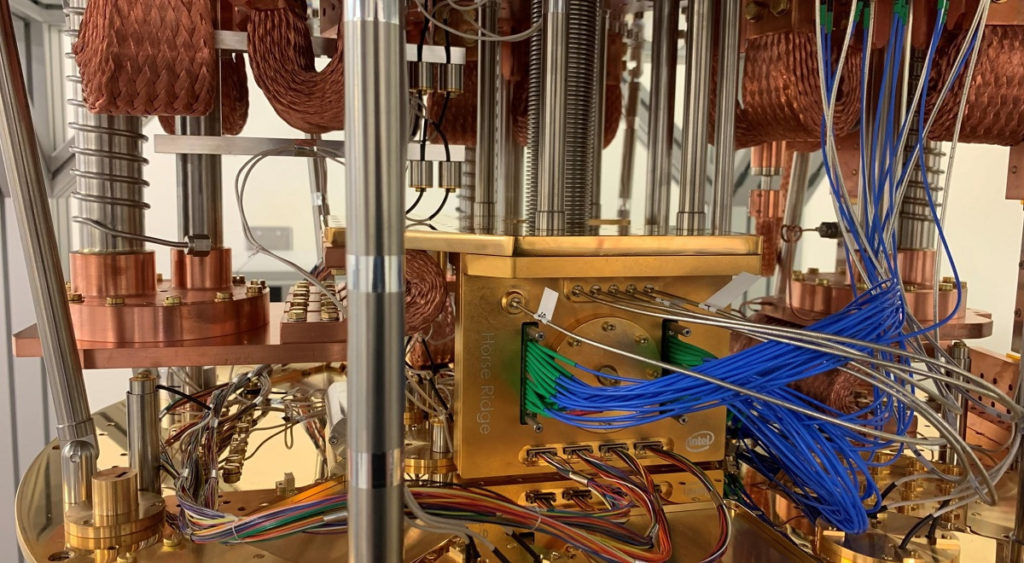
At the outset of the project, Intel’s researchers designed the scalable system-on-chip (SOC) to operate at cryogenic temperatures, simplifying the control electronics and interconnects required to elegantly scale and operate large quantum computing systems. Most quantum computing systems only really works at near-freezing temperatures. Intel is trying to change that, but in the meantime, the control chip eliminates having to run hundreds of wires into a refrigerated case that houses the quantum computer.
Quantum researchers are working with just a small number of qubits, or quantum bits, using smaller, custom-designed systems surrounded by complex control and interconnect mechanisms. Applying quantum computing to real-world problems relies first and foremost on the ability to scale to, and control, thousands of qubits at the same time, with high levels of fidelity.
Increases in qubit count trigger other issues that challenge the capacity and operation of the quantum system. One such potential impact is a decline in qubit fidelity and performance. In developing the original Horse Ridge, Intel optimized the multiplexing technology that enables the system to scale and reduce errors from “phase shift” — a phenomenon that can occur when controlling many qubits at different frequencies, resulting in crosstalk among qubits. The engineers can tune various frequencies leveraged with Horse Ridge with high levels of precision, enabling the quantum system to adapt and automatically correct for phase-shift when controlling multiple qubits with the same radio frequency (RF) line, improving qubit gate fidelity.
With Horse Ridge II, Intel’s researchers have added the ability to manipulate and read qubit states and control the potential of several gates required to entangle multiple qubits, according to a talk by Jim Clarke, director of quantum hardware in Intel’s Components Research Group.
Why it matters
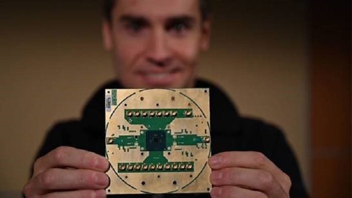
Above: Stefano Pellerano, principal engineer at Intel Labs, holds the original Horse Ridge.
Image Credit: Intel
Intel said that today’s early quantum systems use room-temperature electronics with many coaxial cables that are routed to the qubit chip inside a dilution refrigerator. This is why the chip you see in the image is surrounded by wires and cryogenic cooling systems. This approach does not scale to a large number of qubits due to form factor, cost, power consumption, and thermal load to the refrigeration unit. With the original Horse Ridge, Intel took the first step toward addressing this challenge by eliminating the need for multiple racks of equipment and thousands of wires running into and out of the refrigerator in order to operate the quantum machine. Intel replaced these bulky instruments with a highly integrated system-on-chip (SoC) that simplifies system design and uses sophisticated signal processing techniques to accelerate setup time, improve qubit performance, and enable the engineering team to efficiently scale the quantum system to larger qubit counts.
Horse Ridge II builds on the first-generation SoC’s ability to generate RF pulses to manipulate the state of the qubit, known as qubit drive. It introduces two additional control features, paving the way for further integration of external electronic controls into the SoC operating inside the cryogenic refrigerator.
For instance, a feature called the qubit readout grants the ability to read the current qubit state. The readout is significant, as it allows for on-chip, low-latency qubit state detection without storing large amounts of data, thus saving memory and power. Intel added a programmable microcontroller within the integrated circuit to enable Horse Ridge II to deliver higher levels of flexibility in how the three control functions are executed. The microcontroller uses digital signal processing techniques to perform additional filtering on pulses, helping to reduce crosstalk between qubits.
Intel built Horse Ridge II with a 22-nanometer low-power FinFET manufacturing process. It works at a temperature of 4 kelvins, or minus 452 degrees Fahrenheit. That’s pretty cold, just a fraction above absolute zero.
Silicon spin qubits — the underpinning of Intel’s quantum efforts — have properties that could allow them to operate at temperatures of 1 kelvin or higher, which would significantly reduce the challenges of refrigerating the quantum system. Intel will further describe technical details at the International Solid-State Circuits Conference (ISSCC) in February 2021.
Integrated silicon photonics for datacenters
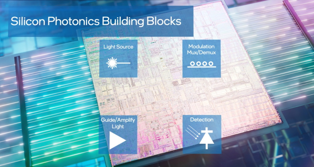
Above: Intel is researching silicon photonics to make datacenters more efficient.
Image Credit: Intel
Meanwhile, Intel also announced progress in integrating photonics with low-cost, high-volume silicon. The advancements represent critical progress in the field of optical interconnects, which address growing challenges around the performance scaling of electrical input/output (I/O) as compute-hungry data workloads increasingly overwhelm network traffic in datacenters. Intel demonstrated advances in key technology building blocks, including miniaturization, paving the way for tighter integration of optical and silicon technologies.
The computing industry is quickly approaching practical limits of electrical input-output (I/O) performance. As bandwidth demand for datacenter compute keeps increasing, electrical I/O isn’t scaling to keep pace, resulting in an “I/O power wall” that limits available power for compute operations. By bringing optical I/O directly into servers and onto chip packages, Intel hopes to break down this barrier, enabling data to move more efficiently.
At the Intel Labs event, the company demonstrated key progress in building blocks, which include light generation, amplification, detection, modulation, complementary metal-oxide semiconductor (CMOS) interface circuits, and package integration — all essential to achieve integrated photonics. A prototype shown at the event featured tight coupling of photonics and CMOS technologies, serving as a proof-of-concept of future full integration of optical photonics with core compute silicon. Intel also showcased micro-ring modulators that are 1,000 times smaller than traditional components. The large size and cost of conventional silicon modulators have been a barrier to bringing optical technology onto server packages, which require the integration of hundreds of these devices. These combined results pave the way for the extended use of silicon photonics beyond the upper layers of the network to inside the server and onto future server packages.
