In this article, we’ll take a high-level look at the process of designing analog ICs.
Analog IC Design vs. Digital IC Design
Contents
Analog IC design differs greatly from digital IC design. Where digital IC design is mostly done at an abstracted level with systems and processes that determine the specifics of gate-/transistor-level placement and routing, analog IC design generally involves more personalized focus into each circuit, and even the sizing and specifics of each transistor.
Also, many foundry processes are primarily developed for digital ICs with analog features, which requires analog IC designers to work with process constraints and features better suited to digital ICs.
Image used courtesy of Rony B Chandran
Design Specification
Analog design teams generally start with a set of specifications and features, much like with digital IC design. From there, functional models of the various functions are used to further narrow down the constraints and lead to decisions on device size, type, and other process features. This may include transistor selections, high-level floorplanning, inclusion of inductor and capacitor technologies, and desired figure-of-merit for the IC and sub-circuits.
Architecture hardware description language (AHDL), such as VHDL-AMS, is used to perform simulations at high levels and determine the constraints of sub-blocks. A test-bench may also be developed at this stage that is later used in simulation, though analog designers also often develop test benches for their sub-circuit designs as well.
Subcircuit Design, Physical Layout, and Simulation
With these details in place and depending on the complexity of the analog circuit, analog design teams typically assign the sub-circuits design to individuals. Idealized macro-level measurements are made that further determine the constraints and performance expectations of the subcircuits.
Following this, these macro-schematics are broken down into schematics with circuit elements modeled from the foundry process. Simulation and optimization of these circuits are performed, and then the physical layout process begins. Placement and routing followed by design rule checks (DRC) and layout versus schematic is done prior to parasitic extraction and post-layout simulation.
A post-layout simulation may reveal flaws in the design and an iterative process of redesign, layout, and simulation may be required to meet the final design goals and submit the IC for tape-out. Sub-circuits may also undergo their own design, layout, and simulation process prior to the entire chip layout and simulation, though either approach can lead to the need to redesign circuits prior to tape-out.
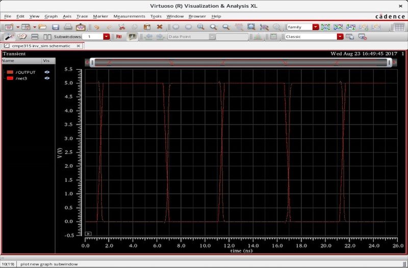
Example of a waveform window of the Cadence Analog Design Environment. Screenshot used courtesy of Saad Rahman and Chintan Patel via the University of Maryland Baltimore County
Analog Abstraction Levels
Below are the abstraction levels of the analog IC design process:
- Functional
- Behavioral
- Macro
- Circuit
- Transistor
- Physical layout
Analog IC Design Flow
The steps associated specifically with analog IC design can be broken down as follows:
- Design specification
- Specifications
- Constraints
- Topologies
- Test bench development
- Schematic flow
- System-level schematic entry
- Architecture HDL simulation
- Block HDL specification
- Circuit-level schematic entry
- Circuit simulation and optimization
- Physical flow
- PCell-based layout entry
- Design rule check (DRC)
- Layout versus schematic (LVS)
- Parasitic extraction
- Post-layout simulation
- Tape-out
In the next article, we’ll talk about the design of RF (radio frequency) integrated circuits.
