Researchers have developed some of the tiniest microsensors to date. Barely visible to the human eye, they can be used for next-generation electronic devices and microprocessors.
A team at Cornell University has developed the nanoscale sensors, which include an integrated circuit, solar cell, and light-emitting diodes (LEDs) all in a device of which 30,000 can fit on one side of a penny.
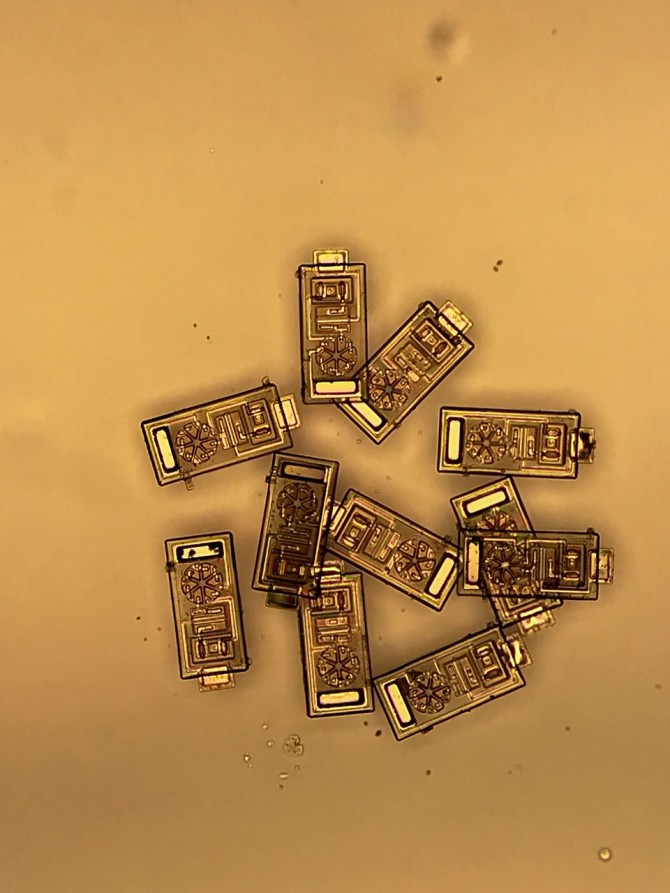 |
| A magnified look at a collection of optical integrated wireless circuits developed by researchers at Cornell University. Typically, these sensors are barely visible to the naked eye. (Image source: Alejandro Cortese) |
The sensors can be used to provide power as well as communication capability in a variety of complex yet lightweight and low-power electronic devices, said Alejandro Cortese, a Cornell postdoctoral fellow who worked on the research.
“We really developed this as a platform so that a lot of people have space to develop new devices, new applications,” he said. “You can potentially fit thousands of transistors on one of these devices. And that means you can increase the range of things the device can sense, how the device communicates out, or its ability to complete more complex tasks.”
The sensors, or optical wireless integrated circuits (OWICs), are basically tiny smartphones that can be customized with various applications, researchers said. However, instead of relying on radio frequency technology, which is how typical smartphones work to communicate, the OWICs use light as a power source and communication medium.
Overcoming Fabrication Challenges
While placing tiny circuits on a silicon wafer for manufacturing is fairly routine in nanotechnology circles, adding LEDs to the technology to provide this capability provided a challenge for researchers, said Paul McEuen, a Cornell professor of physical science who co-led the research with colleague Alyosha Molnar, associate professor of electrical and computer engineering.
LEDs are made with gallium arsenide, a material that has special manufacturing needs because it’s different from silicon. To integrate the LEDs on the silicon wafers with the electrical components used in the sensors, researchers had to develop a complex assembly method using 15 layers of photolithography, 30 different materials and more than 100 steps.
This was especially complex because of the nanoscale on which technicians must work, Cortese noted.
“There are a lot of people working at larger scales where you can pick up things and see them with your eye and touch them,” he said of the task. “This is not that. It’s at a scale that you legitimately cannot see what you’re doing unless you’re under a microscope. So you really have to gain an intuition about the nanoscale and the microscale.”
However, researchers did eventually achieve success with their work, producing up to 1 million OWICs on an eight-inch wafer, which means each device costs a fraction a penny to fabricate.
Applying the Technology
The OWICs, once freed from the silicon, can be used in a number of ways, researchers said. One is to measure inputs like voltage and temperature in hard-to-reach environments, such as inside living tissue and microfluidic systems, they said. An example of this would be using the OWIC with a neural sensor to noninvasively record nerve signals in the body and transmit data using the LED by blinking a coded signal.
The team published a paper on its work in the journal Proceedings of the National Academy of Sciences (PNAS).
To prove their concept, researchers embedded an OWIC with a temperature sensor in brain tissue and wirelessly relayed the results. The results show how the technology can be used to provide complex sensing capability without using the power it typically would require.
To continue the research, as well as to commercialize the OWICs, the team of McEuen, Molnar, and Cortese have launched the company OWiC Technologies and filed a patent for their technology. The first commercial application will be the creation of e-tags that can be attached to products to help identify them.
Elizabeth Montalbano is a freelance writer who has written about technology and culture for more than 20 years. She has lived and worked as a professional journalist in Phoenix, San Francisco and New York City. In her free time she enjoys surfing, traveling, music, yoga and cooking. She currently resides in a village on the southwest coast of Portugal.
