Since the first radio transmission, the size of the radio spectrum has doubled every 30 months, following an exponential increase in data transfer rates in wireless communications. Over the past two decades, it has become clear that photonics can be combined with radio-frequency (RF) engineering to enable the generation of carrier wave signals with very high frequencies of up to the millimeter-wave (30–300GHz) and terahertz (300–3000GHz) frequency ranges. These frequency bands are essential for enabling an increase in wireless data transfer rates to above 100Gb/s. The combination of photonics and high-frequency electronics has evolved into microwave photonics (MWP), owing to the availability of cost-effective telecom-based components such as lasers, modulators, and photodiodes. The ability to use optical fibers to transmit RF signals over long distances to remote antenna units has been critical in the growth of MWP.
Recently, there has been interest in the potential of MWP to enable the seamless convergence of wired (fiber optic) and wireless communication networks in terms of data transfer rates and modulation formats.1 In particular, the growth of fifth-generation (5G) networks—which aim to increase the number of connected devices tenfold, as well as the data transfer rates for the end user—requires such a combination of wired and wireless networks.
We have now succeeded in combining photonics and high-frequency electronics at the chip level, by developing so-called radio frequency light engines. These provide a cost-effective method of achieving the increased bandwidth required for 5G networks. As part of the iPHOS research project funded by the European Commission, in collaboration with III-V Lab and University College, London, we integrated a complete photonic transmitter system in a single chip: see Figure 1. This chip received an electrical input and generated a modulated millimeter-wave electronic signal in a coplanar microstrip line ready for transmission to an antenna.2
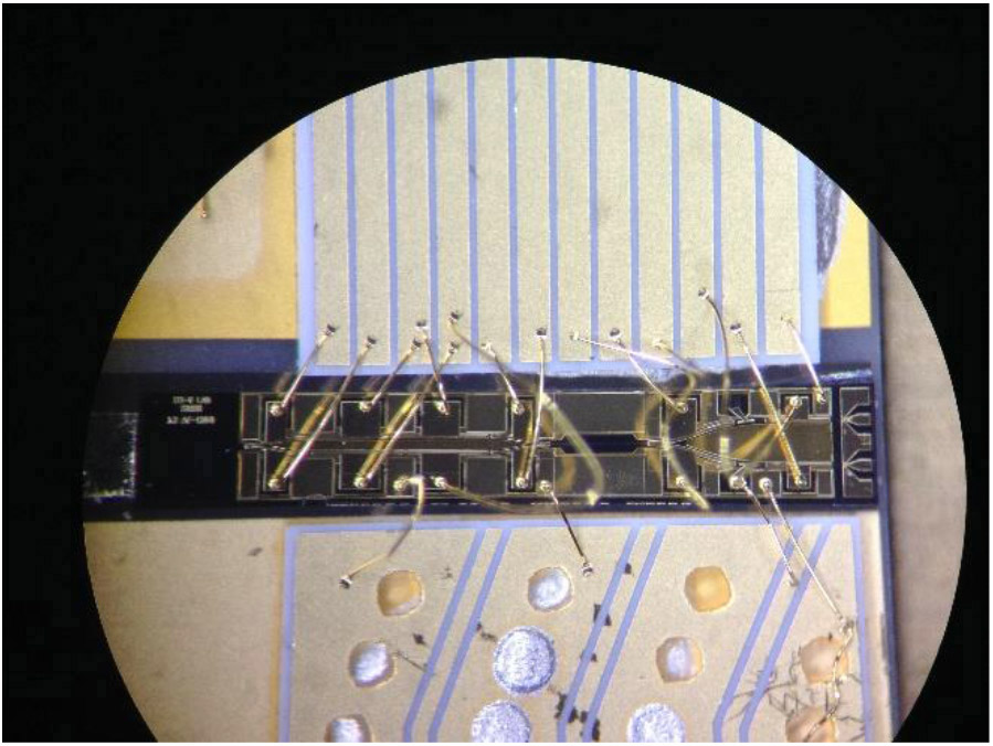
Figure 1. A monolithic indium phosphide photonic integrated circuit for use as a millimeter-wave transmitter chip.
The development of integrated photonic components has been facilitated by the establishment of new facilities in Europe. In particular, collaboration between academia and industry with the support of the European Commission has resulted in multi-project wafer production runs that are commercially available to circuit designers.3 These production runs, which use fabrication foundries, have the advantage that circuit designers can share the costs of the design tools, fabrication processes, and maintenance of the facilities. Each foundry uses a specific material substrate, such as indium phosphide or silicon, has a specific set of components that master onto that substrate, and provides designers with a standardized set of photonic components that are optimized to enable high performance. Using a library of components, we designed a chip that was fabricated at the SMART Photonics foundry: see Figure 2. This chip contains different laser structures that produce optical signals which generate high-frequency electronic signals when used to illuminate a high-speed photodiode. A patent held by NTT for a uni-traveling carrier photodiode is close to expiry,4 which might increase the availability of high-speed photodiodes.
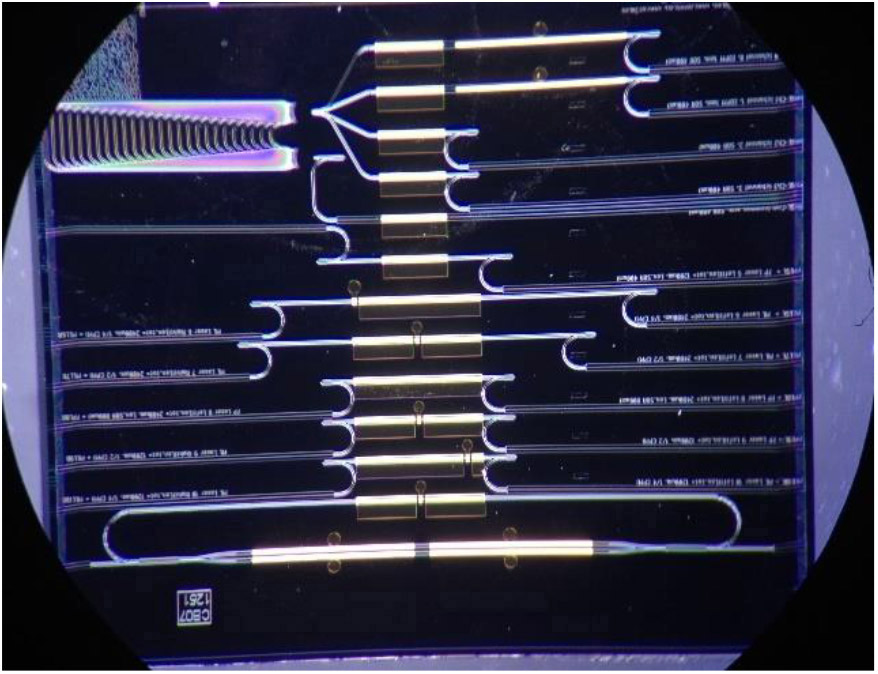
Figure 2. The photonics integrated circuit that we designed, which contains laser devices for the generation of high-frequency signals.
Unfortunately, the integration of broadband antennas onto the substrate materials is hampered by the high dielectric constant of the substrates, which does not allow RF signals to be radiated efficiently. This indicates a need for new integration techniques, as different components require specific sets of material parameters that cannot be achieved using a single substrate. Instead of monolithic integration of all the circuit elements in a single chip, the focus has shifted to heterogeneous or hybrid integration. Heterogeneous integration comprises combining multiple material substrates on a chip-scale form factor to ‘mix and match’ a variety of devices and materials to provide the best substrate for each function. Hybrid integration, on the other hand, involves combining multiple preprocessed chips.
The current focus of hybrid and heterogeneous integration is predominantly on silicon components. However, polymer-based hybrid components have also attracted attention, owing to their potentially low cost and the possibility of integrating in one chip broadly tunable lasers and phase shifters for phased-array transmitters. Also, the low permittivity of polymer materials allows the integration of broadband antennas. Recently, in collaboration with the Fraunhofer Heinrich Hertz Institute (HHI) and Osaka University, we demonstrated the advantages of dual polymer-based distributed Bragg reflector lasers based on the HHI PolyBoard integration structure for generating high frequencies.5
Current pressure to increase data transfer rates in wireless communications is bringing new challenges to photonic integration. We believe that this will result in a diversification of the materials used in integrated devices, instead of the current dominance of silicon-based devices. In addition to the contribution that our chips have made to facilitating the increase in data transfer rates, our future work will focus on the development of high-speed wireless links, which will improve the cost-effectiveness of small cells in 5G networks.
Guillermo Carpintero
Carlos III University of Madrid
Leganés, Spain
Guillermo Carpintero is an associate professor in the Department of Electronic Technology. He has undertaken research into photonic integrated circuits, in particular, the development of integrated optical systems on a chip for applications in microwave photonics.
References:
1. T. Nagatsuma, G. Carpintero, Recent progress and future prospect of photonics-enabled terahertz communications research, IEICE Trans. Electron. E98-C, p. 1060-1070, 2015.
2. G. Carpintero, K. Balakier, Z. Yang, R. C. Guzman, A. Corradi, A. Jimenez, G. Kervella, Microwave photonic integrated circuits for millimeter-wave wireless communications, J. Lightwave Technol. 32, p. 3495-3501, 2014.
3. M. Smit, X. Leijtens, H. Ambrosius, E. Bente, J. van der Tol, B. Smalbrugge, T. de Vries, An introduction to InP-based generic integration technology, Semicond. Sci. Technol. 29, p. 083001, 2014.
4. T. Ishibashi, T. Furuta, N. Shimizu, K. Nagata, Y. Matsuoka, M. Tomizawa, Pin photodiode with improved frequency response and saturation output, US Patent 5818096, 1998.
