Since its proprietary technology launched back in 2014, industrial 3D printer OEM Nano Dimension has built a name for itself in the world of additively manufactured electronics (AME).
With ongoing refinements to its flagship DragonFly LDM® 3D printer, the company is now doubling down on its 3D printing of high-performance electronic devices (Hi-PEDs™), an area in which it’s seen significant success in recent years. The Hi-PEDs™ targeted by the company often cannot be produced using traditional printed circuit board (PCB) manufacturing processes.
Yoav Stern, CEO of Nano Dimension, states, “We’re the 3D printing company for customers who need to stay on the cutting edge of electronics design. You’re creating the latest innovations in hardware development and electronic circuits. You need an additive manufacturing solution that allows you to go where no one has gone before in electronics design — and to get there faster and easier than ever before.”
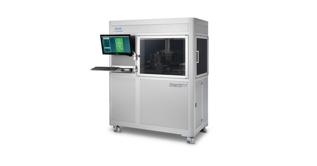
The DragonFly LDM
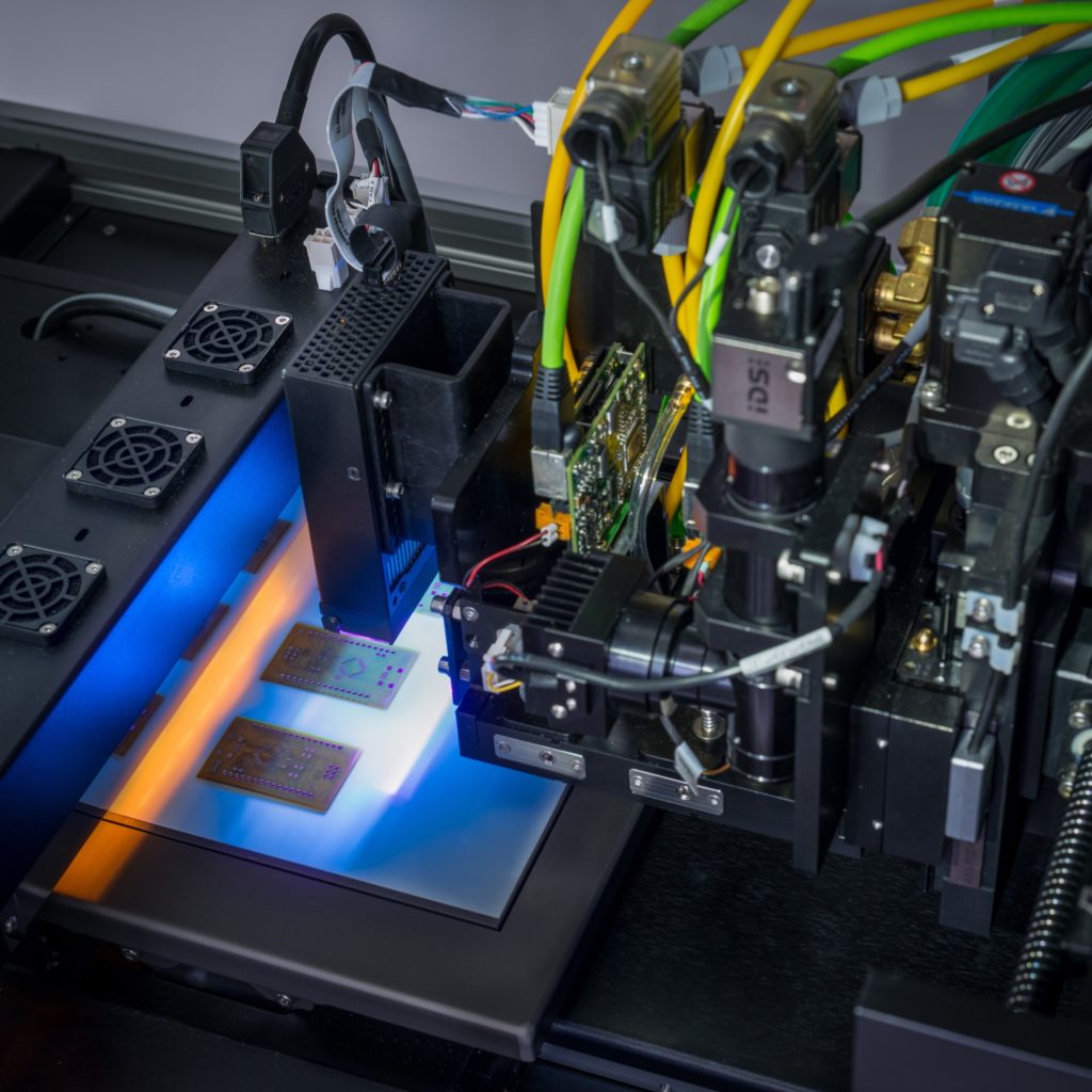
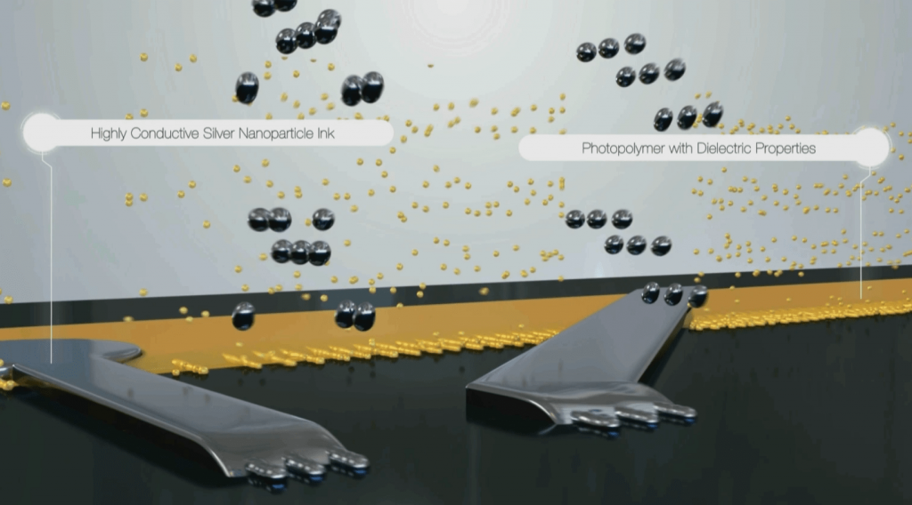
The DragonFly LDM® is the driving force behind Nano Dimension’s AME capabilities, combining freeform geometrics with embedded 3D electronics. Equipped with two individual printheads, the system can simultaneously deposit a conductive silver nano-ink and a dielectric photopolymer ink. The former comprises the bulk of a printed circuit’s connections, while the latter serves to provide mechanical support, thermal resistance, and electrical insulation for the surrounding structure.
Well-suited for rapid prototyping purposes, the system is safe for use in both an office and laboratory environment. Starting with a Gerber or CAD file, the user can produce custom Hi-PEDs™ such as complex multilayer circuits with a couple of clicks. The system’s AME technology allows for many embedded electronic components, including capacitors, antennas, coils, and converters, to name a few. As an aside, the ability to install electronics in non-conventional cubic packages is also possible, whereby they are separate from the rest of the circuit boards.
Stern adds, “Nano Dimension bridges the gap between PCB and semiconductor integrated circuits. A revolution at the click of a button — from CAD to a functional and high-performance AME device in hours, solely at the cost of the consumable materials.”
AME 3D printing for the ISS
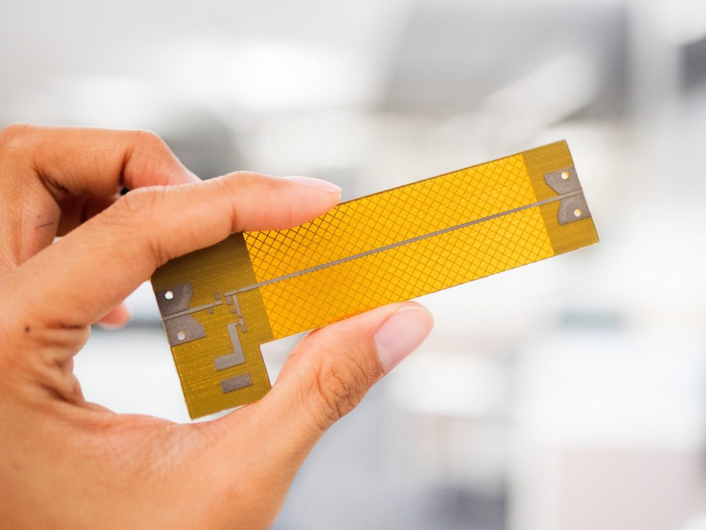
Although the AME process has its uses in many industries, from medical to automotive, one project completed in collaboration with communications technology firm Harris Corporation (now L3Harris) stands out. The partners worked to 3D print a radio frequency (RF) circuit for transmitting data to and from the ISS. RF circuits’ traditional production is usually a very tedious trial and error process, with numerous design iterations.
Dr. Arthur Paolella, a senior scientist for L3Harris, said, “The applications of 3D printing are broad, touching almost every aspect of research, design, and manufacturing. This project’s major objective is to fly an experiment consisting of an integrated communications circuit fabricated by additive manufacturing and analyze those materials’ RF properties in a space environment. As far as we know, this will be the first systematic approach to analyzing such a device in space.”
Having employed Nano Dimension’s AME technology, the partners 3D printed a 101 x 38 x 3mm circuit in around 10 hours. After testing the 3D printed RF circuit against a conventionally manufactured counterpart, L3Harris determined the two had very similar transmission performances. The time and cost differences were really where 3D printing shined as Nano Dimension’s RF circuit allowed for several design iterations in a much shorter space of time, ultimately resulting in reduced costs and a faster time to market.
Subscribe to the 3D Printing Industry newsletter for the latest news in additive manufacturing. You can also stay connected by following us on Twitter and liking us on Facebook.
Looking for a career in additive manufacturing? Visit 3D Printing Jobs for a selection of roles in the industry.
Featured image shows Nano Dimension’s AME technology 3D printing a PCB. Photo via Nano Dimension.
