PHOTO COURTESY OF JOHANSON TECHNOLOGY
Integrated passive components (IPCs) are attracting increasing interest due to the miniaturization of wireless devices, as well as the need to increase reliability of signal conditioning in radio frequency (RF) circuits such as filtering, impedance matching, differential to single-ended conversion, and coupling.
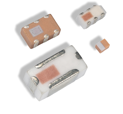
IPCs are electronic sub-systems that combine multiple discrete passive components into a single surface-mounted device. Manufactured using low temperature cofired ceramic (LTCC) technology that allows passive components to be layered in 3D, IPCs deliver the same functionality as 10 to 40 individual components, reducing required board space.
With this approach, the entire front-end between RF chipset and antenna can be manufactured in a single, ultra-low profile (0.35mm to 1.0mm total thickness) package that is less than 20% the size of the same circuit comprised of discrete components.
“If you were to look at the circuit from above, you would only see three chips: the RF wireless chip, the IPC, and the antenna,” explains Manuel Carmona, RF business development and product manager at Johanson Technology. “The design is clean and small. You can make the overall printed circuit board (PCB) size much smaller using IPCs while maintaining high wireless performance.”
IPCs also deliver greater reliability. By creating a circuit within a small LTCC package, variability and potential points-of-failure are nearly eliminated. A single integrated package of matching components also assures compliance with FCC or ETSI requirements.
“A lot of the variability of solo surface-mounted components is due to the individual variance of each component. When you multiply that by 10 to 20 components, you just need one weak link in the RF chain for the entire front-end to fail,” Carmona says.
IPCs are available for almost any type of passive circuit, including low- and high-pass filters, diplexers, triplexers, impedance matched baluns, balun-filters, band pass filters, and couplers.
LTCC technology
Manufacturing IPCs is similar to creating multi-layer surface mounted device (SMD) component parts, such as capacitors and inductors. However, LTCC manufacturing allows circuits to be embedded in up to 40 separate layers of a 3D package that is still very low profile.
Using this manufacturing process, Johanson Technology developed a line of small, highly reliable IPCs for RF systems. These components operate across several bands from 300MHz to 10GHz, covering cellular, DECT, WLAN, Bluetooth, 802.11 (a, b, and g), and GPS applications.
Each integrated package is RF tested to ensure all components are working properly and are fully integrated.
“Because the LTCC manufacturing process is extremely precise and repeatable, we can stay within the manufacturing limits of alignment, variations, and so forth, so you get really consistent, robust RF circuitry,” Carmona says.
Matched-filter baluns
One IPC offering is Johanson Technology’s line of matched-filter baluns.
A balun is an electrical device that converts between a balanced (differential) and unbalanced (single-ended) signal. The component has many forms and may include devices that also transform impedances.
Because many RF wireless chipsets have differential (two pin) outputs – an RF input and output – that connect to a single-ended antenna, the signal must be converted from differential to single-ended in a specific impedance ratio. These wireless radio frequency integrated circuits (RFICs) usually have a non-standard complex impedance that the IPCs match for optimum power efficiency. Some baluns are also combined with bandpass, low-pass, or high-pass filters.
To accomplish an impedance conjugate match, Johanson Technology works with chipset original equipment manufacturers (OEMs) to create specific baluns with matching part numbers for each chip. Reference designs during development simplify and speed up chipset adoption.
Markets
Because IPCs require much less board space, engineers can design miniaturized devices with RF circuitry and create smaller form-factor products.
Beyond size, a smaller PCB can also impact product aesthetics, allowing slim, low profiles. Eliminating components on a 10:1 or greater basis also reduces overall device weight.These factors have major implications for next-generation smart wearables (rings, bracelets, shoes, jeans, shirts, and other apparel), implantable medical devices, and portable electronics.
Johanson Technology
https://www.johansontechnology.com
