In 2020, TSMC saw its net profit rise significantly due to the massive increase in global demand for smartphones, IoT applications, and high-performance computing devices. This demand has led the company to realize its best-ever quarterly financials and increased optimism in research opportunities.
Following a board meeting on February 9, TSMC disclosed its plans to spend roughly $178 million on a Japanese subsidiary to expand its three-dimensional integrated circuit (3D IC) material research.
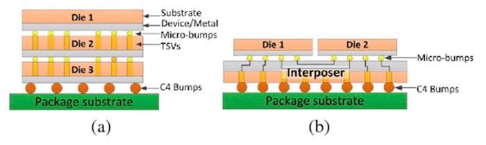
This image shows an example of an (a) 3D IC and a (b) 2.5D IC. Image used courtesy of Y. Xie, Chongxi Bao, Y. Liu, and Ankur Srivastava
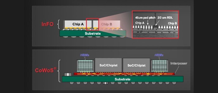
TSMC’s Research Thus Far with 3D ICs and “3DFabric”
TSMC has been working with 3D-IC technology for quite some time. With computing applications and workloads are as demanding as they have ever been, TSMC claims it is leading the way into the third-dimension with “3DFabric.” This fabric is TSMC’s family of “3D silicon stacking and advanced packaging technologies“ designed to complement its semiconductor IP.
An expanded view of TSMC’s “3DFabric.” Image used courtesy of TSMC
At the virtual 2021 International Solid-State Circuits Conference (ISSCC), TSMC’s chairman Mark Liu spoke about 3D system fabrics as the key driver for keeping major technology developments and innovations moving. Liu also highlighted the future of 3D chip stacking with TSMC’s system-on-integrated-circuits (SoIC), in which a dozen dies can be stacked in a vertical space of less than 600 µm thanks to low-temperature bonding.

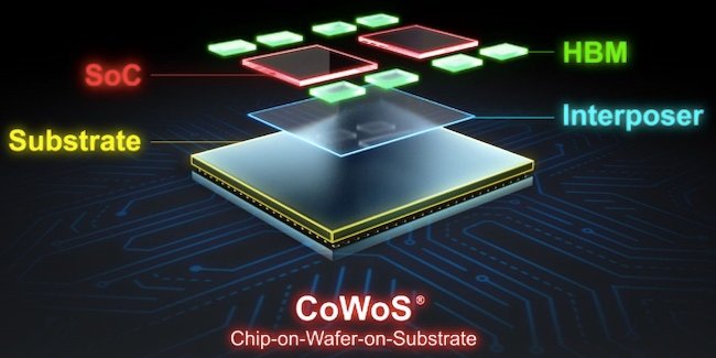
System integration using TSMC’s 3DFabric. Image used courtesy of TSMC
The $178 million USD in funding for TSMC’s Japanese R&D center will expand its efforts in 3D IC material development. Plans for the R&D center are expected to be completed later this year.
3D IC and SoIC
A 3D IC is made by stacking silicon wafers and interconnecting them on different planes to behave as a single device. This method enables better performance metrics with reduced power consumption and a smaller footprint than two-dimensional circuits.
Improvements for 3D-IC technology may open doors to improvements in SoICs. These SoICs can integrate “chiplets” from different SoC parts and with varying functions into a new chip. TSMC also mentions its innovative bonding scheme that provides shorter and faster connections for those chiplets.
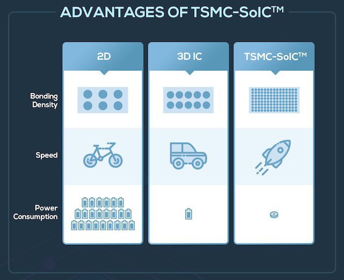
A high-level, simple depiction of the differences between a 2D IC, a 3D IC, and TSMC’s SoIC. Image used courtesy of TSMC
Thus far, TSMC’s research has yielded more advanced, efficient, and flexible ways of using SoCs and creating SoICs. It will be interesting to see where TSMC utilizes its funding to keep the momentum going with 3D IC advancements.
