Download this article in PDF format.
What you’ll learn:
- Characteristics of IGZO-TFT-based circuits that are making them more popular alternatives in design.
- The challenges faced when dealing with AMOLED displays.
- Examples of applications employing IGZO-TFT-based circuits.
Thin-film transistors (TFTs) made of indium-gallium-zinc-oxide (IGZO) as the semiconducting material are typically used in backplane circuits for displays. TFTs offer many complementary features compared to silicon-based transistors, such as processing on large-area glass or flexible substrates, extremely low leakage current in standby mode, ability to drive mixed voltages, and the potential to achieve a lower cost per unit area.
By using silicon-like circuit design flows, IGZO-TFT-based circuits can be designed and integrated into applications beyond displays. These include large-area imagers for fingerprint sensing, printed sensor readout for wearable health patches, RFID tags for connecting physical objects to the Internet of Everything, and many others.
Reading and Driving Sensors and Actuators
Contents
- 1 Reading and Driving Sensors and Actuators
- 2 IGZO-TFT Technology: A True “Flexible Friend”
- 3 Tackling Major Challenges for AMOLED Displays
- 4 Brightness Variation
- 5 Dimming Ability
- 6 A Fingerprint Sensor in Everyday Objects
- 7 A Flexible ECG Patch Compatible with NFC
- 8 Tags and Sensors Communicating with Touchscreens
- 9 From Prototypes to Multi-Project Services
Sensors and actuators are crucial components in present and future IoT solutions because they provide an interface between the analog “real” world and the digital “virtual” world. They sense the real-world environment, while electronic systems make decisions using the sensed data and trigger a response. Think CO2 sensors for air-quality monitoring, infrared sensors for intrusion detection, temperature sensors for health wearables, etc. Audio speakers and displays are well-known examples of actuators. With the increasing prevalence of digital connectivity, sensors and actuators will become more and more ubiquitous.
At the heart of these sensing and actuation systems are readout and driver electronics—electronic circuits that capture the sensor’s analog data or send a drive current or voltage to the actuating element. Today, the readout and driver electronic circuits for almost all of these applications are built using Si-CMOS technology.
TFT technology can offer features that are complementary to Si-CMOS technology. Applications requiring circuit integration on large surface areas, curved surfaces, or flexible forms could well benefit from using TFT technology instead of Si-CMOS technology. Depending on the material used for the semiconductor layer, there are different TFT technologies available, such as amorphous-silicon, IGZO, and low-temperature polysilicon (LTPS). Applications based on IGZO-TFTs are the focus of this article.
IGZO-TFT Technology: A True “Flexible Friend”
IGZO is a semiconductor that can be processed at relatively low temperatures (i.e., below 300°C) on flexible, large-area substrates. IGZO-TFTs have the potential of being low cost due to the simple process flow and material choice.
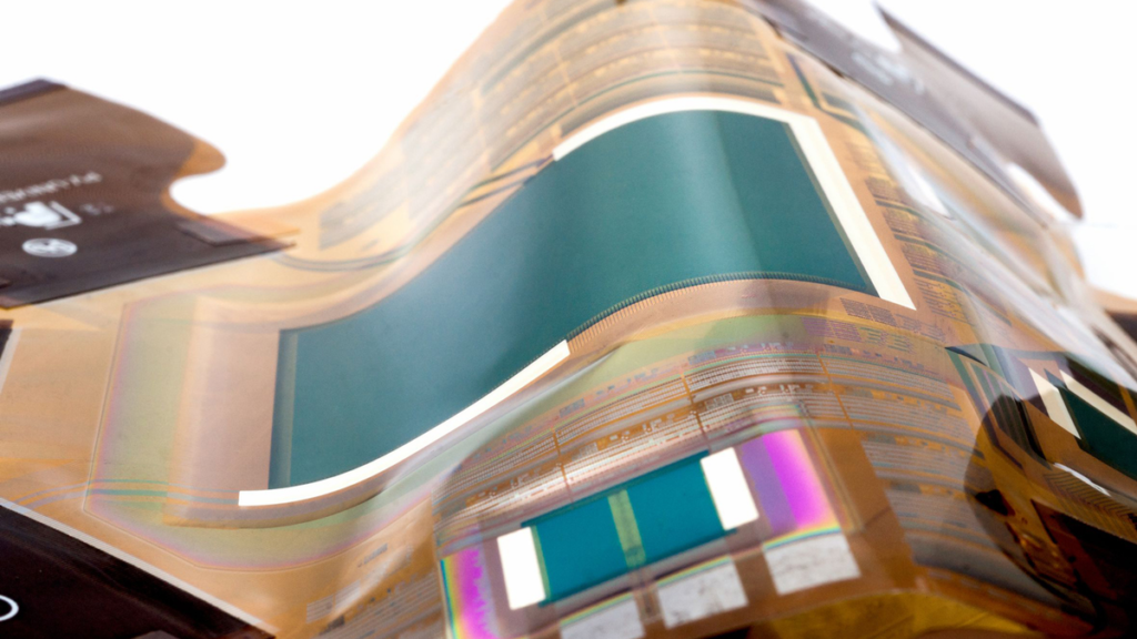
IGZO-TFTs have already found their way into commercial applications serving as backplanes in television and smartphone displays (Fig. 1). Backplanes contain arrays of TFTs that are responsible for switching and driving individual display pixels, therefore acting as a determining factor for display resolution, refresh rate, and power consumption. The display foundries manufacture these backplanes on glass substrates with different dimensions, the largest of which can be up to 3.37 × 2.94 m (required for large televisions, e.g., 65 inches).
![1. Cross-section of a typical IGZO-TFT-based backplane (presented at the 2020 Display Week [1]).](https://rfengineer.net/wp-content/uploads/2020/12/Figure_1___AMOLED_TFT_backplane.5fd0e973c19c9.png) 1. Cross-section of a typical IGZO-TFT-based backplane (presented at the 2020 Display Week [1]).
1. Cross-section of a typical IGZO-TFT-based backplane (presented at the 2020 Display Week [1]).
The device size of IGZO-TFTs fabricated on such large glass plates is typically in the micron range (compared to nanometer-sized Si-CMOS transistors on 300-mm wafers), due to limitations of photolithography equipment and materials available in display foundries. The device size limitation impacts the number of transistors in a pixel.
Besides that, IGZO-TFTs are available as n-type transistors only. Unlike in Si-CMOS technology, there’s no comparable p-type transistor in TFT technology. This challenge makes it difficult to design high-performance analog electronic circuits in TFT technology, which is crucial to readout data from IoT sensor nodes.
The large device sizes limit the switching frequency of IGZO-TFT circuits compared to Si-CMOS circuits. This limitation restricts their application to moderate-frequency applications only (e.g., RFID/NFC requiring 13.56 MHz), and high-frequency applications such as Bluetooth and Wi-Fi are out of scope.
Imec has overcome several of these challenges through innovative circuit designs and has demonstrated the use of IGZO-TFTs for applications beyond display backplanes. Below, we give some examples of sensors and actuators that implement novel IGZO-TFT-based circuits for driving and readout.
Tackling Major Challenges for AMOLED Displays
TFT backplanes in active-matrix organic light-emitting-diode (AMOLED) displays typically implement at least two transistors and one capacitor per pixel, referred to as the 2T1C driving circuit. One of the transistors functions as a select transistor, selecting the pixel when it needs to be active. The other acts as a drive transistor, controlling the current that flows through the OLED element. The capacitor is used as a storage element, storing the pixel’s data (i.e., the analog voltage for the gate of the drive transistor) while it’s being selected.
TFT-driven AMOLED technology has increasingly become popular for mobile devices and television displays due to its improved brightness, thinness, flexibility, and efficiency compared to LCD displays. However, two critical challenges crop up.
Brightness Variation
AMOLED displays are subject to variations in current that flows through the drive transistors. These variations mainly result from dissimilarities in the threshold voltages of small transistors on the display panel. The dissimilarities lead to a variation in brightness, resulting in a non-uniform appearance on the display.
Adding compensation circuits to the driving circuits could help solve the problem. However, doing so would increase the number of transistors and, subsequently, the area needed per pixel, thereby negatively impacting the display resolution. For displays requiring very high resolution, such as augmented-reality (AR) displays, “8K” televisions, or advanced mobile applications, an external compensation method is more desirable.
Imec, in collaboration with KU Leuven and TNO at Holst Centre (the Netherlands), has developed a new compensation principle using the existing 2T1C driving circuit in combination with a peripheral silicon chip. The compensation cycle starts with measuring the current through each pixel for each data voltage. From these measurements, each drive transistor is characterized, and essential transistor parameters are extracted and stored in external memory. Based on these parameters, data voltage can be compensated for local pixel variations for every pixel and frame at different pixels’ grey values.
The operation requires only a limited amount of calculation power. With this compensation method, the teams have demonstrated a significant improvement in electrical and optical uniformity. The calculation time could be reduced to a minimum, making the method applicable to, say, real-time videos.
Dimming Ability
A second challenge relates to the AMOLED display’s ability to provide different brightness levels in different circumstances. In bright daylight, the display will need its full luminance for a good appearance, while in a dark environment, the brightness can be lowered.
For several applications, such as automotive or outdoor mobile applications, dimming must happen quickly, without impacting the display’s resolution or dynamic content. The simplest way to do this is by applying different analog voltages at the drive transistor gate to control the brightness. But the accuracy of such driving schemes heavily depends on the accuracy of the external analog voltage source, which is often limited. Another approach is to switch to digital driving schemes, e.g., by applying a pulse-width-modulation (PWM) signal to drive the OLED, but this method also has its limitations.
Imec, KU Leuven, and TNO at Holst Centre solved this issue by implementing a combination of analog and digital driving—using only the 2T1C driving circuit. In this case, though, the drive transistor uses a second active gate—the backgate—which connects to a global PWM signal used for global brightness dimming.
When the PWM signal is high, the current to the OLED pixel can be controlled by the analog data voltage (Fig. 2). When the PWM signal is low, there’s no current at all. The correct level of brightness can now be obtained by “playing” with the PWM signal’s duty cycle, i.e., the percentage of time the PWM signal is on. With this simple 2T1C driving scheme, upscalable to high-resolution applications, uniform global dimming can be performed without modifying the true colors.
![2. Test image at PWM duty cycle 100% (left), and PWM duty cycle 50% (right) (presented at the 2020 Display Week [2]).](https://rfengineer.net/wp-content/uploads/2020/12/Figure_2___AMOLED_display_dimming.5fd0e993da977.png) 2. Test image at PWM duty cycle 100% (left), and PWM duty cycle 50% (right) (presented at the 2020 Display Week [2]).
2. Test image at PWM duty cycle 100% (left), and PWM duty cycle 50% (right) (presented at the 2020 Display Week [2]).
A Fingerprint Sensor in Everyday Objects
IGZO-TFT circuits, arranged in large backplane arrays, can enable a range of applications “beyond displays.” One example is a flexible fingerprint sensor, where an array of TFTs in the readout circuitry extracts the sensor’s signals.
Fingerprint sensing is increasingly being used for identity protection. Various sensing methods (optical, ultrasound, thermal, etc.) are being explored, each of them bringing different benefits and challenges. Most of the sensors are fabricated on a Si-CMOS platform, making them expensive, rigid, and limited in size. A thin-film technology platform would offer many advantages and allow the sensors to be integrated into everyday curved objects, such as doorknobs and car keys.
An attractive approach for implementing fingerprint sensing makes use of thermal mass detection. The large water content of the skin results in a large thermal mass, while the air trapped inside the valleys of the skin has very little thermal mass. CEA-Leti/Liten (France) brought a method to detect this difference using pyroelectric PVDF-TrFE to the Horizon 2020 PYCSEL project. Collaboration between them, imec, and TNO at Holst Centre brought a demonstration imager to fruition.
The teams designed a dedicated readout system, which starts with injecting an amount of heat in each pixel of the imager. This heat quantum induces a temperature increase, which depends on the thermal mass of the skin and/or valleys. For a given temperature step, a certain amount of charge generated by a pyroelectric material is stored within the pixel. The IGZO-TFT backplane extracts these charges row by row. The charges are then transferred into a readout IC, digitized, processed, and visualized. The fabricated 500-ppi sensor shows good fingerprint image quality, which isn’t affected by delaminating or bending the sensor (Fig. 3).
![3. Photograph of the fingerprint sensor after delamination (presented at the 2020 Display Week [3]).](https://rfengineer.net/wp-content/uploads/2020/12/Figure_3___Fingerprint_sensor.5fd0e9ae0ce64.png) 3. Photograph of the fingerprint sensor after delamination (presented at the 2020 Display Week [3]).
3. Photograph of the fingerprint sensor after delamination (presented at the 2020 Display Week [3]).
A Flexible ECG Patch Compatible with NFC
IGZO-TFT-based circuits in non-backplane configurations can serve applications for which flexibility and/or low cost are key requirements. Think about biomonitoring systems, such as flexible electrocardiogram (ECG) patches, conformable to the human body’s shape. In this application, TFT circuits and the electrode capture analog ECG signals representing the heart’s electrical potentials.
As previously noted, with IGZO-TFTs, it’s challenging to design high-performance analog electronics, such as amplifiers or analog-to-digital converters (ADCs). In addition, IGZO-TFTs are ill-suited for high-frequency communication protocols (Bluetooth or Wi-Fi), making it challenging to transfer data wirelessly to a handheld device or PC.
Imec, in collaboration with TNO at Holst Centre and the Eindhoven University of Technology, demonstrated an ECG sensor with TFT-based circuits optimized for signal acquisition, amplification, and digitalization (Fig. 4). The digitized raw data are transmitted to a smartphone using near-field communication (NFC) for further processing and visualization.
![4. Simulated response of the full system to an ECG source signal (published by nature publishing group, Flexible Electronics [4]).](https://rfengineer.net/wp-content/uploads/2020/12/Figure_4___ECG_patch.5fd0e9c9da7ce.png) 4. Simulated response of the full system to an ECG source signal (published by nature publishing group, Flexible Electronics [4]).
4. Simulated response of the full system to an ECG source signal (published by nature publishing group, Flexible Electronics [4]).
Key innovations in this work are in the signal digitization method and compatibility with NFC radio-frequency (RF) communication. Unlike conventional ADCs, input data are digitized in the time domain by transforming the input signal into a PWM representation and using the NFC radio clock as a reference. The duty cycle of the PWM signal is proportional to the signal amplitude. This time-to-digital converter generates a 105.9-kb/s bit stream, which is compatible with the 13.56-MHz NFC standard.
Tags and Sensors Communicating with Touchscreens
The flexible ECG patch is an excellent example of an IoT sensor that connects to a smartphone using short-range NFC communication, which connects to the cloud. NFC communication needs a dedicated NFC reader, and the NFC tags require integration of the IGZO-TFT NFC chip with the antenna, and that increases cost in terms of antenna printing and assembly. What if we could simply use the smartphone’s touchscreen as the reader interface for sensors and tags? What if we could eliminate the external antenna making it compact and cheaper?
Touchscreens are omnipresent. They can be found in the billions of mobile phones worldwide, and in other emerging touchscreen-enabled devices, such as cars, home appliances, or smart surfaces. Imagine adding personalization or security features to the touch interaction on these touchscreen-enabled devices. For example, in the car, you could use this solution to easily upload your personalized radio settings by simply holding a dedicated tag against the touchscreen.
Teams from imec, KU Leuven, and TNO at Holst Centre recently demonstrated a 64-bit IGZO-based identification tag that capacitively couples to a touchscreen (Fig. 5). The metal lines of the touchscreen and the electrodes of the IGZO-based tag form the capacitor. The glass of the touchscreen acts as part of the dielectric in between the artificial capacitive components.
![5. Application cases of capacitive-coupled tags integrated in cards (presented at the 2020 Display Week [5] and published in Nature Electronics [6]).](https://rfengineer.net/wp-content/uploads/2020/12/Figure_5___CT_tag.5fd0e9e1ecb9d.png) 5. Application cases of capacitive-coupled tags integrated in cards (presented at the 2020 Display Week [5] and published in Nature Electronics [6]).
5. Application cases of capacitive-coupled tags integrated in cards (presented at the 2020 Display Week [5] and published in Nature Electronics [6]).
When the tag touches the smartphone, the subsequent touch event can be compared with swiping a finger across the touchscreen. The capacitive-coupled touchscreen tag creates a swipe from the first electrode to the next, and the coordinates are processed by the app in the smartphone to decode the transmitted code.
From Prototypes to Multi-Project Services
An innovative IGZO-TFT circuit design is the critical element in all of the above examples. With its many years of designing and fabricating IGZO-TFT based electronic circuits, imec can help companies and academic research groups explore the possibilities of such circuits for their applications and products. Besides IGZO-TFTs, imec also has experience in designing LTPS-TFT-based circuits.
Imec and TNO at Holst Centre have been strategically collaborating for several years on thin-film electronics R&D and have leveraged the GEN1 IGZO R&D line at TNO at Holst Center for joint projects, including the projects on fingerprint sensors and capacitive tags mentioned in this article. The Interreg Flexlines project has enabled a development and prototyping service at the GEN1 IGZO line for future requests.
Besides in-house R&D, imec is currently setting up collaborations with commercial fabs to offer design and manufacturing of TFT-based circuits for display and non-display applications. This model is being set up in concert with multi-project services that have existed for years for Si CMOS-based technologies, offering academia and application companies a path from R&D to manufacturing.
For some of these developments, the teams partially received funding from the European Research Council (ERC) under the European Union’s Horizon 2020 research and innovation programme:
- Under grant agreement N° 732423 (PYCSEL project), for the fingerprint sensor.
- Under grant agreement N° 716426 (FLICS project), for the ECG sensor and CT tag.
- Under grant agreement N° 732389 (CAPID project), for the CT-tag.
The work was also financed by the Flexlines project within the Interreg V-program Flanders-The Netherlands, a cross-border cooperation program with financial support from the European Regional Development Fund, and co-financed by the Province of Noord-Brabant, The Netherlands.
More detailed information on these IGZO-TFT-based circuits can be found in the following papers:
[1] “A 2T1C AMOLED display with external compensation reducing on-panel current variations to 0.079%,” by L. Verschueren et al, presented at the 2020 Display Week. [2] “AMOLED display global dimming using PWM on backgate,” by L. Verschueren et al, presented at the 2020 Display Week. [3] “Flexible large-area multi-fingerprint sensors based on thermal mass detection,” F. De Roose et al, presented at the 2020 Display Week. [4] “A flexible ECG patch compatible with NFC RF communication,” M. Zulqarnain et al, nature publishing group, Flexible Electronics, 2019. [5] “IGZO-based identification tags communicating with everyday touchscreens,” N. Papadopoulos et al, presented at the 2020 Display Week. [6] “Touchscreen tags based on thin-film electronics for the Internet of Everything,” N. Papadopoulos et al, Nature Electronics, 2020.To find out about access to these papers, go here.
