By Jim Martens and David Zima
The IoT has increased the demand for good radio frequency (RF) design practices from the mains, to wall outlet power, all the way to the antenna. With several IoT standards employed today, constraint management has become critical to ensuring that designs meet product performance and reliability.
Even the simplest of IoT designs can benefit from constraint management. RF constraint management helps PCB designers and engineers understand and meet new challenges and requirements, such as how to comply with regulatory certification and how to avoid overlooking something that may lead to failed tests at compliance test time.
As long time users of Mentor’s PADS RF layout tools, RF Laboratories, Inc., recently added the PADS Professional creation platform to its toolkit.
A single integrated constraint management environment ensures that design intent is maintained. With comprehensive physical and time-based constraints, PADS Professional equips PCB engineers and designers with correct-by-construction capabilities that help you achieve greater innovation, eliminate costly re-spins and get products to market faster.
In this article, we will describe how best practices combined with RF constraint management and layout techniques help us reduce design iterations and speed up design time of RF PCBs for the IoT, as well as other applications.
A well-conceived and executed RF layout involves a deliberate and self-conscious effort at constraining all design artwork to be devoid of pitfalls and strictly adhere to high-frequency design rules. Simply put, by systematically limiting the design scope before we start, constraints make it more likely that we will produce a successful layout for a given design. In other words, constraints guide the design and implementation of the layout toward meeting both IoT standards and design requirements.

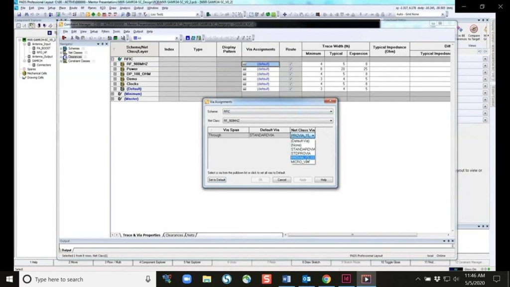
Fig. 1: Constraint Manager screen.
Good PCB design practices reduce the potentially undesirable affects on transmission lines and the resulting EMI issues. The first thing you need to do is ask a set of questions that will help you understand and implement constraint assignments before using your constraint manager.
- What’s the highest frequency and what’s the fastest time in the system?
- What are the electrical specifications at the inputs and outputs of the syncs and the sources?
- Are there sensitive signals to route—for example, controlled impedances, propagation delays on traces, or clock-distribution buses?
- Is there a microstrip that would solve a problem or do you need to use a strip line and bury it?
- How many different supply voltages exist? And can those supply voltages be put in different groups?
- Does each supply voltage need its own power plane or is it possible to split them?
With all these questions answered, you are now ready to begin using PADS Professional to assign and manage constraints.
One of the most important aspects affecting layout is the location of each functional block. PADS Professional easily handles grouping similar nets that have similar parameters, such as speed, time of flight, and all of the other items covered in the previous section.
Once you have created a diagram of the functional groups of your system (transmitter path, receiver path, analog signals, digital signals, and so forth), assigning constraints is much easier.
When assigning constraints, one of the first things to look for are interconnections between two or more independent functional groups, as these may result in crosstalk problems. To avoid crosstalk, you need to understand the PCB manufacturer’s specifications regarding minimum width separation, minimum distance between two layers, and minimum drill requirements for vias. Finally, it may seem obvious, but do not forget to make sure that your choices are permitted for your design and its target prices, not to mention whether your board house can accomplish the mechanical requirements.
What is the best way to understand and address these considerations? A good place to start is the board stackup. The board Stackup Editor is very useful in helping you configure the optimal board stackup. This is especially beneficial because there is no hard rule about how many layers should be used and how the board stackup should look. A complete ground plane in high-speed designs is essential. A complete power plane is recommended as well. Although the best solution is for every voltage to have its own layer and its own ground plane, it is not practicable nor affordable and would result in a huge number of layers, so that’s not an option. The RF IC pictured in figure 2 has four layers: a primary (top) layer, a copper plane layer, a ground plane layer, and a bottom layer.

Fig. 2: PADS Professional Stackup Editor.
You need at least two layers when using microstrip traces: a power plane and a ground plane. Microstrip traces are used for sensitive signals, with a complete power plane as close as possible to the ground plane. It’s possible to create capacity with coupling between them to get low impedance at high frequencies. This reduces the amount of impedance on small decoupling capacitors at the power pins of the devices. The closer the planes, the less impedance is present.
Placing decoupling capacitors between the power pin and ground pin of a device ensures low AC impedance to reduce noise and store energy. To reach low impedance over a wide frequency range, several capacitors have to be used. This is why a real capacitor behaves as a resonant circuit, consisting of its capacitance and its parasitic inductance and resistance. Therefore RF IoT designs typically have two or more capacitors in parallel to obviate high-frequency noise issues.
Vias are essential in most routing layouts, but you have to be careful when using them. Vias add additional inductance and capacitance, and reflections can occur due to changes in the characteristic impedance. Thus, vias also increase the trace length. PADS Professional Constraint Manager is very helpful in handling vias. The Via Assignment setting allows you to simply select and assign a via that would be appropriate for a particular RF trace, including blind and buried vias that go from one layer of the board to another.
It’s important to remember that right angles in a trace can cause higher radiation. The capacitance increases in the region of the corner and the characteristic impedance changes. This impedance causes reflections, so you want to avoid right-angle bends in a trace. Try to route them with at least 45-degree corners to minimize any impedance changes. Even better, route using arcs, which are one of the many RF-centric layout features available in PADS Professional.
You’ll also want to separate high-speed signals from low-speed signals and digital signals from analog signals. One way to do this is by routing such traces at 90 degrees to one another on different layers, instead of in parallel, and you can minimize crosstalk by doing the same. Also, avoid vias in differential traces. If it’s not possible to avoid them, then use vias in both traces or compensate for the delay in one of the traces in the other.
Finally, clock distribution networks should have minimal delays. Above all you want to avoid branches to reduce reflections. Use a clock driver to distribute the signal in every device and pay close attention to proper termination.
Understanding good RF layout practices is essential for designing RF designs for the IoT. Best practices combined with RF constraint management and layout techniques using PADS Professional has proven to be a recipe for successful RF layout at RF Laboratories, Inc.
To get more technical background on this topic, please download David Zima’s new paper How RF Laboratories Accelerates RF PCB Design for IoT with Constraint Management. You can also view Mr. Zima’s reference design centered presentation on RF constraint management techniques in the on-demand seminar Save Time Using Constraint Management – A Success Story from RF Laboratories, Inc.
 David Zima is the president and principal RF/Microwave design engineer at RF Laboratories, Inc. Zima’s technical background covers many areas, including RF and microwave hardware design, antenna design, regulatory compliance/EMI, H-field backscatter, bio-medical telemetry, embedded software and wireless contract manufacturing. Zima is a BSEE, CCEMTP, and holds an FCC General Radiotelephone Operators License with Radar Endorsement.
