Welcome to our high-level IC design flow series! Below, you will find the introduction to the series and links to the individual series parts.
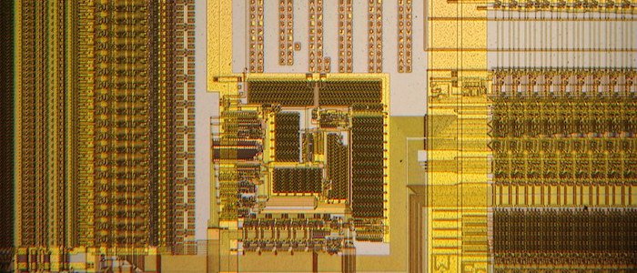
A look inside the famous Intel 486 DX IC. Image used courtesy of yellowcloud. [CC BY 2.0]
Contents
What Is an IC Design Flow?
IC design flow is the process of developing an IC design to the point at which the IC can be manufactured in a semiconductor fabrication plant (i.e., a foundry). This involves the use of sophisticated device and process models, as well as mathematical tools and software to capture, simulate, optimize, and detect errors during the process.
The knowledge and expertise of engineers, technicians, and designers alongside modern electronic design automation (EDA) or computer-aided design (CAD) tools are key aspects in transforming product and circuit concepts into production-ready IC designs.
Types of IC Design
Though the exact IC design flow may be different for each foundry, process, company, design group, and even individual, there are four main domains where the IC design flow process can be broken down. These domains are:
- Digital
- Analog
- RF
- Mixed-signal
Each domain has several distinct features, where Mixed-signal Design Flow may be an amalgamation of any combination of the Digital, Analog, or RF domains.
Digital IC design encompasses all IC design that purely uses transistors as switches and logic circuits. Conversely, Analog IC design includes all IC design that involves real-world signals that haven’t been digitized. RF IC Design, considered by some to be a subset of Analog IC Design, includes working with signals beyond several hundred kilohertz where RF phonomena dominate the design constraints and techniques.
A Note on PDKs (Process Design Kits) and EDA Tools
The differences in the design flow of the domains can, and often do, extend from the early concept phases all the way to production. However, there are increasingly more ICs built that include circuitry from each domain, which leads to much more complex and nuanced processes. Due to this evolution, foundries and EDA tool companies often work to make foundry processes and EDA tools more compatible.
Many foundries build process design kits (PDKs) for their customers to use, which include data files used by IC design EDA software tools to aid with design flow. The elements in these data files often consist of parameterized cells (PCELLS), SPICE models, schematic symbols, parasitic extraction tools, DRC/LVS tools, technology data, and various scripts. Some design companies also contract or build their own scripts and tools to automate and enhance verification features.
The following sections provide an overview of the IC design flow for each domain listed above, and a discussion of mixed-signal IC design flow and interaction of the domains in modern ICs and electronics.
The IC Design Flow Basics Series
You can find the sections below:
