Samsung made headlines last week when it announced the availability of its newest 3D IC technology.
The new technology, called X-Cube, was tested and proven in a 7nm test chip, which stacked SRAM on top of a logic chip. The result was a smaller footprint and shorter signal paths, meaning faster signal propagation and less power consumption. X-Cube is also available in advanced nodes: both 7nm and 5nm.
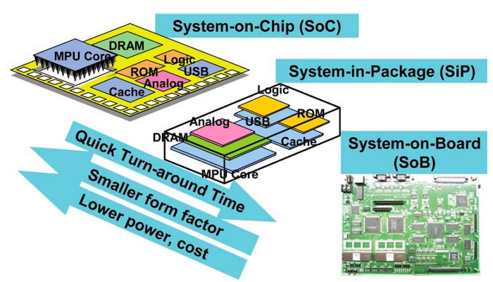
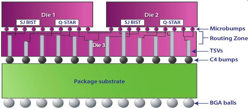
Comparison in SoC, SiP, and SoB. Image used courtesy of Resve Salah et al.
Contents
This advance from Samsung addresses several trends in chip design: facing the end of Moore’s law, increasing chip functionality, and addressing the difficulties of systems-on-chip (SoCs).
The Issue With Increasing SoC Size
One of the major challenges in SoC design is the fact that integrating more functional blocks onto one chip requires significantly more chip area.
But the combination of greater chip area and subsequently smaller node sizes leads to a huge rise in interconnect parasitics. Longer wire lengths must be used to connect different blocks in a physically larger chip, which increases interconnect inductance.
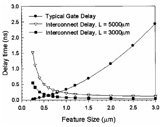
Sources of delay based on feature size and interconnect length. Image used courtesy of Parag Gadarki
The increased parasitic impedance of interconnects has come with a slew of problems. Data movement energy—the energy consumed from the physical movement of data on-chip—becomes one of the largest sources of energy consumption.
Signal propagation delay is also negatively affected by increased wire length and interconnects parasitic. Yet, with Moore’s law coming to an end, designers have to think of new ways to increase chip speed without scaling down in a conventional manner.
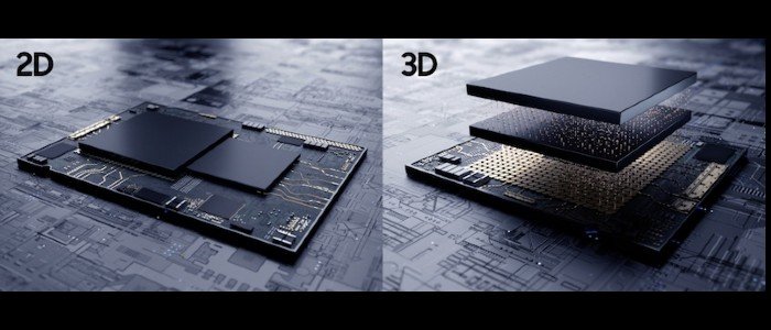
The Solution: 3D ICs
To allow chips to continually expand in size while overcoming these aforementioned issues, designers have turned to 3D IC technology. 3D ICs are unique in that they physically stack silicon wafers or dies on top of each other.
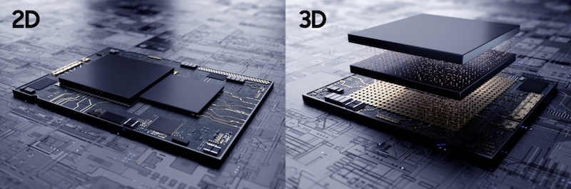
3D IC technology illustration. Image used courtesy of Samsung
Each wafer on a 3D IC is connected with a through-silicon via (TSV). In this way, chips can continue to grow in size—but instead of growing longer and wider in 2D, they grow taller in 3D, saving board area.
The Benefits of 3D ICs
3D ICs offer many benefits over conventional, large-area SoCs, most of which stem from shortening the interconnect. With functional blocks stacked on top of each other and connected through TSVs as opposed to long wires like in a 2D SoC, 3D ICs are able to significantly decrease interconnect length.
Most notably, decreasing the interconnect length helps alleviate parasitic impedances in the interconnect, which in turn allows for decreased propagation delay (i.e faster operation) and less data movement energy (i.e less power consumption).
3D IC technology using TSVs. Image used courtesy of Ridgetop Group
The other obvious benefit of 3D ICs is the ability to densely integrate large functionality into smaller areas, offering a good alternative to the end of Moore’s law. It’s worth noting that this dense integration also comes with drawbacks such as increased power density and thermal management issues.
Samsung Introduces Accessible 3D IC Tech
Samsung’s news may mark the beginning of advanced and accessible 3D IC technologies. Moonsoo Kang, senior VP of foundry market strategy at Samsung Electronics says, “Samsung’s new 3D integration technology ensures reliable TSV interconnections even at the cutting-edge EUV process nodes.”
He adds, “We are committed to bringing more 3D IC innovation that can push the boundaries of semiconductors.”
In the future, Samsung plans to build on the initial design, collaborating with global fabless customers to deploy 3D IC solutions in next-generation high-performance applications, like mobile smartphones, AR/VR, wearables, and high-performance computing platforms.
