 Dallas Invents is a weekly look at U.S. patents granted with a connection to the Dallas-Fort Worth-Arlington metro area. Listings include patents granted to local assignees and/or those with a North Texas inventor. Patent activity can be an indicator of future economic growth, as well as the development of emerging markets and talent attraction. By tracking both inventors and assignees in the region, we aim to provide a broader view of the region’s inventive activity. Listings are organized by Cooperative Patent Classification (CPC).
150 patents granted Ranked No. 9 in patent production out of 250 metros
NO. OF PATENTS BY CLASSIFICATION
A: HUMAN NECESSITIES 8
B: PERFORMING OPERATIONS; TRANSPORTING 23
C: CHEMISTRY; METALLURGY 2
E: FIXED CONSTRUCTIONS 5
F: MECHANICAL ENGINEERING; LIGHTING; HEATING; WEAPONS; BLASTING 6
G: PHYSICS 45
H: ELECTRICITY 54
DESIGN: 6
TOP LOCAL ASSIGNEES (NO. OF PATENTS)
Texas Instruments Inc. (Dallas) 25
Sandisk Technologies (Addison) 11
Toyota Motor Engineering Manufacturing North America Inc. (Plano) 9
Micron Technology Inc. (Boise, ID) 5
Bell Helicopter Textron Inc. (Fort Worth) 4
Capital One Services LLC (McLean, VA) 4
Halliburton Energy Services, Inc. (Houston) 4
Futurewei Technologies Inc. (Plano) 3
STMicroelectronics Inc. (Coppell) 3
UNASSIGNED 11
TOP LOCAL INVENTOR (NO. OF PATENTS)
Benjamin L. Weatherford (Princeton) 2
Clifton S. Thompson (Lucas) 2
Dale Robert Anderson (Colleyville) 2
Glen Raggio (Mesquite) 2
Harish N. Venkata (Allen) 2
Ilesh V. Patel (Euless) 2
Thomas Mast (Carrollton) 2
William T. Bigbee Jr. (Melissa) 2
Don’t miss Dallas Invents: Sign up for the Dallas Innovates e-newsletter.
Patent information is provided by Joe Chiarella, founder of patent analytics company Patent Index and publisher of The Inventiveness Index. For additional details on the patents granted below, search the USPTO Patent Full-Text and Image Database.
UTILITY PATENTS
H U M A N N E C E S S I T I E S
Surgical personal protection apparatus
Patent No. 10874163
Inventor(s): Marshall Proulx (Keller, TX)
Assignee(s): Stryker Corporation (Kalamazoo, MI)
Law Firm: Howard Howard Attorneys PLLC (4 non-local offices)
Application No., Date, Speed: 16208630 on 12/04/2018 (756 days app to issue)
Abstract: A personal protection system for providing a sterile barrier around medical/surgical personnel. The system includes a helmet over which a hood or a toga suspended. A microphone, an amplifier and a speaker are mounted to the helmet. Speech of the individual wearing the personal protection system is picked up by the microphone and amplified speech is broadcast by the speaker. The speaker is outwardly directed so as to broadcast the speech out through the hood or toga covering the helmet.
[A41D] OUTERWEAR; PROTECTIVE GARMENTS; ACCESSORIES (eye or ear protectors A61F 9/00, A61F 11/00; sweating suits A61H 36/00)
Motorized surgical instrument
Patent No. 10874382
Inventor(s): Sudhir Prem Srivastava (Frisco, TX)
Assignee(s): SS INNOVATIONS CHINA CO., LTD. (Zhejiang, , CN)
Law Firm: No Counsel
Application No., Date, Speed: 15038478 on 11/21/2014 (2230 days app to issue)
Abstract: In one embodiment of the invention, a motorized surgical instrument including an elongated shaft, a wrist member and a pair of working members with at least one working member moveable relative to other working member between open and closed position, is presented. The elongate shaft includes towards its proximal end a carriage plate that enables independent and controlled motion of the surgical instrument employing plurality of actuators securely held therein. Further, disclosed is a surgical instrument enabling easy and quick replacement of working members.
[A61B] DIAGNOSIS; SURGERY; IDENTIFICATION (analysing biological material G01N, e.g. G01N 33/48)
Tissue release instrument and methods of use
Patent No. 10874414
Inventor(s): John Early (Dallas, TX)
Assignee(s): NEXTREMITY SOLUTIONS, INC. (Warsaw, IN)
Law Firm: Heslin Rothenberg Farley Mesiti P.C. (2 non-local offices)
Application No., Date, Speed: 16107726 on 08/21/2018 (861 days app to issue)
Abstract: A device for releasing soft tissue includes a distractor and blade assembly. The distractor may include a guide channel positioned along an edge of the distractor and the blade assembly fits into the guide channel and is configured to slide within the channel of the distractor.
[A61B] DIAGNOSIS; SURGERY; IDENTIFICATION (analysing biological material G01N, e.g. G01N 33/48)
Deformable dynamization device
Patent No. 10874434
Inventor(s): Alexander M. Cherkashin (Flower Mound, TX), John D. Ross (Ovilla, TX), Mikhail L. Samchukov (Coppell, TX)
Assignee(s): TEXAS SCOTTISH RITE HOSPITAL FOR CHILDREN (Dallas, TX)
Law Firm: Haynes and Boone, LLP (Local + 13 other metros)
Application No., Date, Speed: 15787327 on 10/18/2017 (1168 days app to issue)
Abstract: Dynamization devices and methods of use are provided. A dynamization device may comprise first and second modules that are mated together in a substantially cylindrical shape. The outer surface of the first and second modules are connected to deformable rings that may be deformed when a longitudinal force is applied to the first and second modules. The deformation of the rings creates a longitudinal mechanical bias in the device to return it to its original shape. The strength, spring coefficient, and size of the dynamization device can be adjusted depending upon the particular needs of the application.
[A61B] DIAGNOSIS; SURGERY; IDENTIFICATION (analysing biological material G01N, e.g. G01N 33/48)
Wearable massager
Patent No. 10874579
Inventor(s): Reginald Rembert (Flower Mound, TX)
Assignee(s): UNASSIGNED
Law Firm: No Counsel
Application No., Date, Speed: 15067488 on 03/11/2016 (1754 days app to issue)
Abstract: A wearable massager includes a plurality of attachments, each of which is designed for a specific body part. Each attachment includes at least one massaging module on an inner surface that is either formed of mechanical rollers that simulate a massage as they are moved vertically and horizontally, or a plurality of contiguous, inflatable bladders that simulate a massage as they are inflated and rapidly deflated. A controller allows a user to vary the speed and intensity with which the rollers are moved horizontally and vertically, or the level, order and frequency in which each bladder is inflated and deflated. Accordingly, the continuous movement of the rollers or inflation and deflation of the bladders against the wearer”s skin simulates the typical movements of a massage therapist”s hands and fingers.
[A61H] PHYSICAL THERAPY APPARATUS, e.g. DEVICES FOR LOCATING OR STIMULATING REFLEX POINTS IN THE BODY; ARTIFICIAL RESPIRATION; MASSAGE; BATHING DEVICES FOR SPECIAL THERAPEUTIC OR HYGIENIC PURPOSES OR SPECIFIC PARTS OF THE BODY (electrotherapy, magnetotherapy, radiation therapy, ultrasound therapy A61N)
Compound to treat Sjogren”s syndrome
Patent No. 10874741
Inventor(s): Mark Tengler (Southlake, TX)
Assignee(s): Spectrix Therapeutics, LLC (Southlake, TX)
Law Firm: Chalker Flores, LLP (Local)
Application No., Date, Speed: 16114955 on 08/28/2018 (854 days app to issue)
Abstract: The present invention includes compositions and methods for providing a therapeutically acceptable dose of an active pharmaceutical agent for once a day delivery of the active pharmaceutical compound in an amount effective to treat at least one of: Sjogren”s syndrome, Xerostomia, dry mouth, hypo-salivation, or dental carries due to reduced or compromised salivation, wherein both the peak and trough times in the blood level at 8 hours is greater than 25% of the peak value in the blood level concentration.
[A61K] PREPARATIONS FOR MEDICAL, DENTAL, OR TOILET PURPOSES (devices or methods specially adapted for bringing pharmaceutical products into particular physical or administering forms A61J 3/00; chemical aspects of, or use of materials for deodorisation of air, for disinfection or sterilisation, or for bandages, dressings, absorbent pads or surgical articles A61L; soap compositions C11D)
Sterile patch pump
Patent No. 10874792
Inventor(s): Connor Meehan (Richardson, TX), Lopa Patel (Irving, TX)
Assignee(s): FLEXTRONICS AP, LLC (San Jose, CA)
Law Firm: Volpe Koenig (4 non-local offices)
Application No., Date, Speed: 16134691 on 09/18/2018 (833 days app to issue)
Abstract: An apparatus and method for the aseptic delivery of a biologic medication in a wearable form factor. The apparatus and method allow for standard off-the-shelf drug cartridges to be utilized without compromising the sterility of the biologic. Further, by utilizing a two part assembly, manufacturing costs are minimized.
[A61M] DEVICES FOR INTRODUCING MEDIA INTO, OR ONTO, THE BODY (introducing media into or onto the bodies of animals A61D 7/00; means for inserting tampons A61F 13/26; devices for administering food or medicines orally A61J; containers for collecting, storing or administering blood or medical fluids A61J 1/05); DEVICES FOR TRANSDUCING BODY MEDIA OR FOR TAKING MEDIA FROM THE BODY (surgery A61B; chemical aspects of surgical articles A61L; magnetotherapy using magnetic elements placed within the body A61N 2/10); DEVICES FOR PRODUCING OR ENDING SLEEP OR STUPOR [5]
Holder
Patent No. 10880423
Inventor(s): Aslam Ajani (Dallas, TX)
Assignee(s): UNASSIGNED
Law Firm: No Counsel
Application No., Date, Speed: 16453726 on 06/26/2019 (552 days app to issue)
Abstract: A holder is provided. The holder includes a base, a platform, a first leg, and a second leg. The platform includes a fastener for attaching an object to the platform. The first leg is hingeably coupled to the base and the platform. The second leg is also hingeably coupled to the platform. Each of the first leg and the second leg has a first section and a second section that are hingeably coupled to each other.
[A47B] TABLES; DESKS; OFFICE FURNITURE; CABINETS; DRAWERS; GENERAL DETAILS OF FURNITURE (jointing of furniture F16B 12/00)
O P E R A T I O N S & T R A N S P O R T
Sorbent composition for an electrostatic precipitator
Patent No. 10874975
Inventor(s): David Lyons (Fort Worth, TX)
Assignee(s): S. A. Lhoist Recherche et Developpement (Ottignies-Louvain-la-Neuve, , BE)
Law Firm: Whitaker Chalk Swindle Schwartz PLLC (2 non-local offices)
Application No., Date, Speed: 16032152 on 07/11/2018 (902 days app to issue)
Abstract: A powdery calcium-magnesium compound used as a sorbent composition in flue gas treatment, compatible with electrostatic precipitators. The calcium magnesium compound is doped with calcium nitrate or nitric acid to reduce the electrical resistivity of the particles, increasing their collection efficiency.
[B01D] SEPARATION (separating solids from solids by wet methods B03B, B03D, by pneumatic jigs or tables B03B, by other dry methods B07; magnetic or electrostatic separation of solid materials from solid materials or fluids, separation by high-voltage electric fields B03C; centrifuges B04B; vortex apparatus B04C; presses per se for squeezing-out liquid from liquid-containing material B30B 9/02) [5]
Methods for making oxygen reduction reaction catalysts formed of platinum alloy nanoparticles embedded in porous carbon
Patent No. 10875015
Inventor(s): Hisao Kato (Aichi, , JP), Hongfei Jia (Ann Arbor, MI), Kan Huang (Farmington Hills, MI), Li Qin Zhou (Okemos, MI), Tomoyuki Nagai (Ann Arbor, MI), Xiaochen Shen (Akron, OH), Zhenmeng Peng (Hudson, OH)
Assignee(s): Toyota Motor Engineering Manufacturing North America, Inc. (Plano, TX)
Law Firm: Darrow Mustafa PC (2 non-local offices)
Application No., Date, Speed: 16139936 on 09/24/2018 (827 days app to issue)
Abstract: Methods for making porous materials having metal alloy nanoparticles formed therein are described herein. By preparing a porous material and delivering the precursor solutions under vacuum, the metal precursors can be uniformly embedded within the pores of the porous material. Once absorption is complete, the porous material can be heated in the presence of one or more functional gases to reduce the metal precursors to metal alloy nanoparticles, and embed the metal alloy nanoparticles inside of the pores. As such, the metal alloy nanoparticles can be formed within the pores, while avoiding surface wetting and absorption problems which can occur with small pores.
[B01J] CHEMICAL OR PHYSICAL PROCESSES, e.g. CATALYSIS, COLLOID CHEMISTRY; THEIR RELEVANT APPARATUS (processes or apparatus for specific applications, see the relevant places for these processes or apparatus, e.g. F26B 3/08) [2]
Apparatuses and methods for modifying a defect in a surface
Patent No. 10875071
Inventor(s): Jared R. Hitch (Flemingsburg, KY)
Assignee(s): Toyota Motor Engineering Manufacturing North America, Inc. (Plano, TX)
Law Firm: Dinsmore Shohl LLP (14 non-local offices)
Application No., Date, Speed: 15624188 on 06/15/2017 (1293 days app to issue)
Abstract: An apparatus for modifying a defect in a surface may include a hollow shaft including a first open end and a second open end opposite the first open end, a plunger slidable within the hollow shaft and extending from the first open end, a driver coupled to the second open end of the hollow shaft and extending from the second open end, and a passive resistance mechanism coupling the plunger to the hollow shaft. The passive resistance mechanism biases the plunger towards the second open end of the hollow shaft. The plunger has markings thereon that are visible when the plunger is extended from the first open end. Methods for using the apparatus to modify a defect in a surface are also described.
[B21D] WORKING OR PROCESSING OF SHEET METAL OR METAL TUBES, RODS OR PROFILES WITHOUT ESSENTIALLY REMOVING MATERIAL; PUNCHING METAL (working or processing of wire B21F)
Wall mounted display board system with a base castor and method of use
Patent No. 10875352
Inventor(s): Dony Dawson (Fort Worth, TX), Jeffrey R. Weilert (Fort Worth, TX), Stephen Savoie (Keller, TX)
Assignee(s): UNASSIGNED
Law Firm: Eldredge Law Firm, LLC (2 non-local offices)
Application No., Date, Speed: 15979760 on 05/15/2018 (959 days app to issue)
Abstract: A wall mounted display board system includes a frame; a hinging system to mount on a wall surface and engage with the frame; a panel mounted on a front of the frame; and a castor mounted on a bottom portion of the frame to rest on a ground surface; the hinging system allows the frame and panel to pivot; and pivoting of the hinging system and the frame moves the castor along the ground surface.
[B43L] ARTICLES FOR WRITING OR DRAWING UPON; ACCESSORIES FOR WRITING OR DRAWING (workshop equipment for marking-out work B25H 7/00; teaching hand-writing or drawing G09B 11/00)
Variable compressor control for vehicle air conditioning
Patent No. 10875386
Inventor(s): Daniel B. Gidcumb (West Bloomfield, MI), David W. Cosgrove (Royal Oak, MI), Hidekazu Hirabayashi (Ann Arbor, MI), Stefan Young (Ann Arbor, MI)
Assignee(s): Toyota Motor Engineering Manufacturing North America, Inc. (Plano, TX)
Law Firm: Darrow Mustafa PC (2 non-local offices)
Application No., Date, Speed: 15244426 on 08/23/2016 (1589 days app to issue)
Abstract: A vehicle heating, ventilating, and air conditioning (HVAC) system having a variable compressor can reduce a load applied to a vehicle powertrain during certain conditions. Systems and methods can determine if a power state of an HVAC system is activated, and whether an engine water temperature meets a forced HVAC recirculation intake threshold. Responsive to determining that the engine water temperature meets the forced HVAC recirculation intake threshold, a recirculation mode air source can be selected for the HVAC system. Responsive to the recirculation mode air source being selected, determining if at least one measured vehicle condition meets predetermined criteria. Responsive to determining that the at least one measured vehicle condition meets the predetermined criteria, the variable compressor can be operated according to a reduced duty map.
[B60H] ARRANGEMENTS OR ADAPTATIONS OF HEATING, COOLING, VENTILATING, OR OTHER AIR-TREATING DEVICES SPECIALLY FOR PASSENGER OR GOODS SPACES OF VEHICLES
Tonneau cover with integrated drying cavity
Patent No. 10875392
Inventor(s): Paxton S. Williams (Milan, MI), Scott Louis Frederick (Brighton, MI)
Assignee(s): Toyota Motor Engineering Manufacturing North America, Inc. (Plano, TX)
Law Firm: Darrow Mustafa PC (2 non-local offices)
Application No., Date, Speed: 16395805 on 04/26/2019 (613 days app to issue)
Abstract: A tonneau cover for a vehicle cargo includes a first panel having a first opening structured to enable fluid communication between a first side of the first panel and a second side of the first panel opposite the first side. The tonneau cover defines at least one airflow passage in fluid communication with the first opening and extending along the second side of the first panel.
[B60J] WINDOWS, WINDSCREENS, NON-FIXED ROOFS, DOORS, OR SIMILAR DEVICES FOR VEHICLES; REMOVABLE EXTERNAL PROTECTIVE COVERINGS SPECIALLY ADAPTED FOR VEHICLES (fastening, suspending, closing, or opening of such devices E05)
Door assemblies including vented weather strips and vehicles incorporating the same
Patent No. 10875395
Inventor(s): Brendan R. Dodge (South Lyon, MI)
Assignee(s): Toyota Motor Engineering Manufacturing North America, Inc. (Plano, TX)
Law Firm: Dinsmore Shohl LLP (14 non-local offices)
Application No., Date, Speed: 16239867 on 01/04/2019 (725 days app to issue)
Abstract: A door assembly includes a door frame, a weather strip, and a window glass. The door frame defining a window opening. The weather strip is coupled to the door frame along a portion of the window opening. The weather strip includes an inner flange, an outer flange, and a base that defines a cavity. The inner flange includes a plurality of inner apertures and the outer flange includes a plurality of outer apertures. The window glass is movably coupled to the door frame between a closed position and a vent position. In the closed position the window glass is engaged within the cavity between the plurality of inner apertures and the plurality of outer apertures to inhibit ventilation of air through the weather strip. In the vent position an upper edge of the window glass is engaged within the cavity to permit ventilation of air through the weather strip.
[B60J] WINDOWS, WINDSCREENS, NON-FIXED ROOFS, DOORS, OR SIMILAR DEVICES FOR VEHICLES; REMOVABLE EXTERNAL PROTECTIVE COVERINGS SPECIALLY ADAPTED FOR VEHICLES (fastening, suspending, closing, or opening of such devices E05)
Combination child seat and blanket
Patent No. 10875425
Inventor(s): Wilson Ashu (Fort Worth, TX)
Assignee(s): UNASSIGNED
Law Firm: No Counsel
Application No., Date, Speed: 16282625 on 02/22/2019 (676 days app to issue)
Abstract: A child seat includes a horizontal seat panel and a vertical backrest panel that are each respectively received within a designated compartment in the seat and backrest of an existing passenger seat. Upon command, actuators displace both panels from their designated compartments to form a child seat when needed. A blanket is stored within a pocket mounted on the rear surface of the existing backrest to comfort a passenger. The blanket includes sleeves that allow the passenger to use the arms while covered, an opening for receiving a passenger seat headrest and an inflatable neck pillow encircling a head aperture.
[B60N] VEHICLE PASSENGER ACCOMMODATION NOT OTHERWISE PROVIDED FOR (furniture construction A47)
Adaptive belt for impact
Patent No. 10875494
Inventor(s): Aamir F. Jafri (Little Elm, TX)
Assignee(s): Safran Seats USA LLC (Gainesville, TX)
Law Firm: Kilpatrick Townsend Stockton LLP (14 non-local offices)
Application No., Date, Speed: 16348009 on 08/08/2017 (1239 days app to issue)
Abstract: An adaptive belt is attached to a vehicle seat and includes a first section ([b]101[/b]), a second section ([b]102[/b]), and a third section ([b]103[/b]). The adaptive belt includes a retracted configuration and a fully extended configuration. In the retracted configuration, the adaptive belt is folded between the first section and the second section such that a first attachment attaches the first section to a first portion of the second section. In the retracted configuration, the adaptive belt is also folded between the second section and the third section such that a second attachment attaches a second portion of the second section to a first portion of the third section. In the fully extended configuration, all of the attachments fail thereby increasing a length of the adaptive belt. In response to a threshold loading condition, the adaptive belt changes from the retracted configuration to the fully extended configuration.
[B60R] VEHICLES, VEHICLE FITTINGS, OR VEHICLE PARTS, NOT OTHERWISE PROVIDED FOR (fire prevention, containment or extinguishing specially adapted for vehicles A62C 3/07)
Vehicle occupant authentication system
Patent No. 10875499
Inventor(s): Philip A. Weaver (Plano, TX)
Assignee(s): UNASSIGNED
Law Firm: No Counsel
Application No., Date, Speed: 14858161 on 09/18/2015 (1929 days app to issue)
Abstract: A method is disclosed that is implemented by a computing device in a vehicle. Identifying information is obtained from an occupant of the vehicle via an input device operatively connected to the computing device. If the computing device has connectivity to a remote authentication server, the computing device transmits a request to the authentication server, and controls whether full operation of the vehicle is enabled or disabled based on a response from the remote authentication server. The request includes the identifying information and a vehicle identifier of the vehicle, and requests that the authentication server determine, based on the identifying information and the vehicle identifier, whether the occupant is authorized to operate the vehicle. If the computing device lacks connectivity to the remote authentication server, full operation of the vehicle is temporarily enabled until the computing device has connectivity to the remote authentication server.
[B60R] VEHICLES, VEHICLE FITTINGS, OR VEHICLE PARTS, NOT OTHERWISE PROVIDED FOR (fire prevention, containment or extinguishing specially adapted for vehicles A62C 3/07)
Hopper car double doors
Patent No. 10875548
Inventor(s): Lee A. Reitz (Euless, TX)
Assignee(s): TRINITY RAIL GROUP, LLC (Dallas, TX)
Law Firm: Baker Botts, LLP (Local + 6 other metros)
Application No., Date, Speed: 15978620 on 05/14/2018 (960 days app to issue)
Abstract: According to some embodiments, a railcar comprises a center sill extending along a longitudinal centerline of the railcar, and two side sills. The two side sills are on opposite sides of, and extend parallel with, the center sill. The railcar further comprises a first inner discharge door coupled to the railcar proximate the center sill on a first sick of a longitudinal centerline of the railcar (first side); a second inner discharge door coupled to the railcar proximate the center sill on a second side of the longitudinal centerline (second side); a first outer discharge door coupled proximate the side sill on the first side; a second outer discharge door coupled proximate the side sill on the second side; a first linkage coupling the first inner discharge door to the second outer discharge door; and a second linkage coupling the second inner discharge door to the first outer discharge door.
[B61D] BODY DETAILS OR KINDS OF RAILWAY VEHICLES (vehicles in general B60; adaptation of vehicles to special systems B61B; underframes B61F)
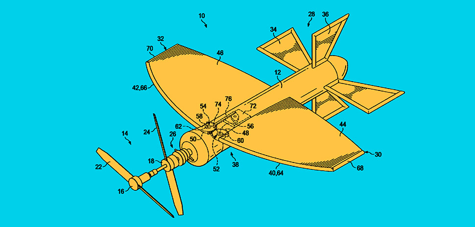
Foldable wings for UAS having a geared interface
Patent No. 10875626
Inventor(s): Dakota Charles Easley (Dallas, TX), Danielle Lynn Moore (Fort Worth, TX)
Assignee(s): Textron Innovations Inc. (Providence, RI)
Law Firm: Lawrence Youst PLLC (Local)
Application No., Date, Speed: 16148005 on 10/01/2018 (820 days app to issue)
Abstract: A foldable wing system for an unmanned aerial system having a fuselage includes a left wing frame having an inboard gear rotatably coupled to the fuselage, a right wing frame having an inboard gear rotatably coupled to the fuselage and a wing actuator coupled to a linkage point on at least one of the wing frames. The wing frames are movable between a plurality of positions including a deployed position and a stowed position. The inboard gear of the left wing frame is engaged with the inboard gear of the right wing frame such that the wing frames move symmetrically between the plurality of positions in response to movement of the linkage point by the wing actuator.
[B64C] AEROPLANES; HELICOPTERS (air-cushion vehicles B60V)
Movable cover for a proprotor nacelle
Patent No. 10875627
Inventor(s): Abey Kurikesu (Fort Worth, TX), Amarjit O. Kizhakkepat (Fort Worth, TX)
Assignee(s): Bell Helicopter Textron Inc. (Fort Worth, TX)
Law Firm: Timmer Law Group, PLLC (1 non-local offices)
Application No., Date, Speed: 15968649 on 05/01/2018 (973 days app to issue)
Abstract: An aircraft, including a fixed nacelle disposed on a wing of the aircraft, the fixed nacelle including a nacelle opening; a proprotor pylon disposed on the wing and rotatable relative to the fixed nacelle between a substantially horizontal position and a non-horizontal position, wherein rotation of the proprotor pylon to a non-horizontal position exposes the nacelle opening; and a movable cover disposed on at least one of the wing and fixed nacelle, said movable cover including a plurality of cover members that are movable between a closed position where at least a portion of the cover members collectively form a protective cover in front of the nacelle opening when the proprotor pylon is positioned in the non-horizontal position and a stowed position where at least a portion of the plurality of cover members are stowed. In other aspects, there is provide a method of covering a nacelle opening.
[B64C] AEROPLANES; HELICOPTERS (air-cushion vehicles B60V)
Skid landing gear assembly
Patent No. 10875633
Inventor(s): John C. Larkin, III (Bristol, TN), Michael R. Smith (Colleyville, TX)
Assignee(s): Bell Helicopter Textron Inc. (Fort Worth, TX)
Law Firm: Timmer Law Group, PLLC (1 non-local offices)
Application No., Date, Speed: 15894888 on 02/12/2018 (1051 days app to issue)
Abstract: An aspect provides a skid landing gear assembly including a cross member disposed between a first skid tube and a second skid tube, and a tension cable member configured to be disposed in the cross member; wherein the tension cable member resists outward deflection of at least a portion of the skid landing gear assembly when a downward load is applied to the skid landing gear assembly. In other aspects, there are methods of avoiding ground resonance in a skid landing gear assembly, methods of assembling a skid landing gear assembly, methods of operating a helicopter with a skid landing gear assembly, and methods of improving the service life of a skid landing gear assembly.
[B64C] AEROPLANES; HELICOPTERS (air-cushion vehicles B60V)
Variable-pitch ringed rotors for aircraft
Patent No. 10875636
Inventor(s): Albert Gerard Brand (North Richland Hills, TX), Eric Albert Sinusas (Southlake, TX), Thomas C. Parham, Jr. (Colleyville, TX)
Assignee(s): Textron Innovations Inc. (Providence, RI)
Law Firm: Lightfoot Alford PLLC (1 non-local offices)
Application No., Date, Speed: 16196950 on 11/20/2018 (770 days app to issue)
Abstract: A rotor system for a rotorcraft has a hub rotatable about an axis and a plurality of blades coupled to the hub for rotation therewith about the axis. Each blade is capable of rotation about a pitch axis relative to the hub, and a ring couples adjacent blades to each other.
[B64C] AEROPLANES; HELICOPTERS (air-cushion vehicles B60V)
De-ice fairing bond fixture
Patent No. 10875638
Inventor(s): David Littlejohn (Haslet, TX), Scott Oren Smith (Bedford, TX), Sven Roy Lofstrom (Irving, TX)
Assignee(s): SIKORSKY AIRCRAFT CORPORATION (Stratford, CT)
Law Firm: Foley Lardner LLP (Local + 13 other metros)
Application No., Date, Speed: 15282263 on 09/30/2016 (1551 days app to issue)
Abstract: A bond fixture includes a first frame defining a chamber configured to receive a leading edge of a rotor blade and a second frame pivotally coupled to the first frame. The second frame is movable between a first position and a second position. In the second position, the second frame restricts movement of the bond fixture relative to the rotor blade. At least one supporting assembly extends from the first frame towards the chamber. The at least one supporting assembly is adjustable to apply a pressure to an adjacent surface of the rotor blade.
[B23K] SOLDERING OR UNSOLDERING; WELDING; CLADDING OR PLATING BY SOLDERING OR WELDING; CUTTING BY APPLYING HEAT LOCALLY, e.g. FLAME CUTTING; WORKING BY LASER BEAM (making metal-coated products by extruding metal B21C 23/22; building up linings or coverings by casting B22D 19/08; casting by dipping B22D 23/04; manufacture of composite layers by sintering metal powder B22F 7/00; arrangements on machine tools for copying or controlling B23Q; covering metals or covering materials with metals, not otherwise provided for C23C; burners F23D)
Mast lockout systems for tiltrotor aircraft
Patent No. 10875640
Inventor(s): Charles Hubert Speller (Flower Mound, TX), Troy Cyril Schank (Keller, TX)
Assignee(s): Textron Innovations Inc. (Providence, RI)
Law Firm: Lawrence Youst PLLC (Local)
Application No., Date, Speed: 15897310 on 02/15/2018 (1048 days app to issue)
Abstract: A mast lockout system for a tiltrotor aircraft having a proprotor assembly. The system includes a mast coupled to and rotatable with the proprotor assembly. A proprotor gearbox having a proprotor gearbox housing is operable to transmit torque and rotation energy to the mast. A lock assembly has first and second lock members. The first lock member is coupled to and rotatable with the mast. The second lock member is coupled to the proprotor gearbox housing. The lock assembly has a first position in which the first and second lock members are disengaged, thereby allowing rotation of the proprotor assembly. The lock assembly has a second position in which the first and second lock members are engaged, thereby preventing rotation of the proprotor assembly. The lock assembly is actuatable between the first and second positions.
[B64C] AEROPLANES; HELICOPTERS (air-cushion vehicles B60V)
Bi-folding engine cowl having a plurality of open positions to provide access
Patent No. 10875656
Inventor(s): Brent Scannell (Roxboro, , CA), Thomas Mast (Carrollton, TX)
Assignee(s): BELL HELICOPTER TEXTRON INC. (Fort Worth, TX)
Law Firm: Patent Capital Group (Local + 6 other metros)
Application No., Date, Speed: 15706338 on 09/15/2017 (1201 days app to issue)
Abstract: In one embodiment of the present disclosure, there is provided an aircraft having a bi-folding cowl for providing full access to equipment without completely removing the cowl. The bi-folding cowl has an upper portion and a lower portion mechanically connected along the adjacent edges, where the upper and lower portions fold so that the inner surfaces face each other when opened. In another embodiment, the bi-folding cowl has at least three maintenance positions, including partially-opened, fully-opened, and fully-opened, lying flat on the surface of the aircraft.
[B64D] EQUIPMENT FOR FITTING IN OR TO AIRCRAFT; FLYING SUITS; PARACHUTES; ARRANGEMENTS OR MOUNTING OF POWER PLANTS OR PROPULSION TRANSMISSIONS IN AIRCRAFT
Hold open j-track locking mechanism for cowling
Patent No. 10875657
Inventor(s): Brent Scannell (Roxboro, , CA), Thomas Mast (Carrollton, TX)
Assignee(s): BELL HELICOPTER TEXTRON INC. (Fort Worth, TX)
Law Firm: Patent Capital Group (Local + 6 other metros)
Application No., Date, Speed: 15706366 on 09/15/2017 (1201 days app to issue)
Abstract: In one embodiment of the present disclosure, there is provided an aircraft that includes a cowling having a j-track mounted on the inwardly facing surface and a rod pivotally connected to a stationary part of the aircraft at a first end and moveable within the j-track at a second end, so that, when the cowling is opened, the second end moves to lock into the j-shaped portion and hold the cowling open. In various embodiments, the first end may be pivotally connected to the aircraft by a quick release pin, and the second end may be connected to the j-track by a torsion spring. In another embodiment of the present disclosure, the cowling is a bi-folding cowl having an upper portion and a lower portion, where the rod and the lower portion may include structures for retaining the lower portion in an opened position.
[B64D] EQUIPMENT FOR FITTING IN OR TO AIRCRAFT; FLYING SUITS; PARACHUTES; ARRANGEMENTS OR MOUNTING OF POWER PLANTS OR PROPULSION TRANSMISSIONS IN AIRCRAFT
Interlocking part transfer cassettes
Patent No. 10875715
Inventor(s): Randy L. Pfeiffer (Dexter, MI)
Assignee(s): Toyota Motor Engineering Manufacturing North America, Inc. (Plano, TX)
Law Firm: Dinsmore Shohl LLP (14 non-local offices)
Application No., Date, Speed: 16445987 on 06/19/2019 (559 days app to issue)
Abstract: A transfer cassette including a base plate, an interlock assembly, a securement plate, and a plate tab. The interlock assembly is arranged on a first edge of the base plate and includes a support arranged on the base plate and a locking finger rotatably arranged on the support. The securement plate is arranged on a second edge of the base plate, opposite the first edge. The plate tab is partially secured to and extending from the base plate.
[B65G] TRANSPORT OR STORAGE DEVICES, e.g. CONVEYORS FOR LOADING OR TIPPING, SHOP CONVEYOR SYSTEMS OR PNEUMATIC TUBE CONVEYORS (packaging B65B; handling thin or filamentary materials, e.g. paper sheets or thread, B65H; cranes B66C; portable or mobile lifting or hauling appliances, e.g. hoists, B66D; devices for lifting or lowering goods for loading or unloading purposes, e.g. fork-lift trucks, B66F 9/00; emptying bottles, jars, cans, casks, barrels or similar containers, not otherwise provided for, B67C 9/00; delivering or transferring liquids B67D; filling or discharging vessels for liquefied, solidified or compressed gases F17C; pipe-line systems for fluids F17D)
System and method for automated truck loading
Patent No. 10875727
Inventor(s): Tim Criswell (Grand Prairie, TX)
Assignee(s): Daifuku Co.. LTD. (Osaka, , JP), Wynright Corporation (Hobart, IN)
Law Firm: Griggs Bergen LLP (Local)
Application No., Date, Speed: 16505407 on 07/08/2019 (540 days app to issue)
Abstract: An automatic case loader for loading product in a trailer is disclosed. A mobile base structure provides a support framework for a drive subassembly, conveyance subassembly, an industrial robot, a distance measurement sensor, and a control subassembly. Under the operation of the control subassembly, product advances through a powered transportation path to an industrial robot which places the product within the trailer. The control subassembly coordinates the selective articulated movement of the industrial robot and the activation of the drive subassembly based upon the distance measurement sensor detecting objects within a detection space, dimensions of the trailer provided to the control subassembly, and dimensions of the product provided to the control subassembly.
[B65G] TRANSPORT OR STORAGE DEVICES, e.g. CONVEYORS FOR LOADING OR TIPPING, SHOP CONVEYOR SYSTEMS OR PNEUMATIC TUBE CONVEYORS (packaging B65B; handling thin or filamentary materials, e.g. paper sheets or thread, B65H; cranes B66C; portable or mobile lifting or hauling appliances, e.g. hoists, B66D; devices for lifting or lowering goods for loading or unloading purposes, e.g. fork-lift trucks, B66F 9/00; emptying bottles, jars, cans, casks, barrels or similar containers, not otherwise provided for, B67C 9/00; delivering or transferring liquids B67D; filling or discharging vessels for liquefied, solidified or compressed gases F17C; pipe-line systems for fluids F17D)
Stackable wire-dispensing container
Patent No. 10875737
Inventor(s): Benjamin L. Weatherford (Princeton, TX), Clifton S. Thompson (Lucas, TX), William T. Bigbee, Jr. (Melissa, TX)
Assignee(s): Encore Wire Corporation (McKinney, TX)
Law Firm: Warren Rhoades LLP (1 non-local offices)
Application No., Date, Speed: 16789365 on 02/12/2020 (321 days app to issue)
Abstract: An apparatus for dispensing wire or cable, the apparatus including an enclosure with a top and a bottom portion and at least three side portions of a first height, a plurality of holes located in both the top and bottom portions of the enclosure, and a core of a second height located within the enclosure, wherein the core forms an area, wherein at least one of the plurality of holes has a first hole diameter and is located in the top and bottom of the enclosure and is located within the area formed by the core, and wherein the wire or cable is placed around the core.
[B65H] HANDLING THIN OR FILAMENTARY MATERIAL, e.g. SHEETS, WEBS, CABLES
Stackable wire-dispensing container
Patent No. 10875738
Inventor(s): Benjamin L. Weatherford (Princeton, TX), Clifton S. Thompson (Lucas, TX), William T. Bigbee, Jr. (Melissa, TX)
Assignee(s): Encore Wire Corporation (McKinney, TX)
Law Firm: Warren Rhoades LLP (1 non-local offices)
Application No., Date, Speed: 16790153 on 02/13/2020 (320 days app to issue)
Abstract: An apparatus for dispensing wire or cable, the apparatus including an enclosure with a top and a bottom portion and at least three side portions of a first height, a plurality of holes located in both the top and bottom portions of the enclosure, and a core of a second height located within the enclosure, wherein the core forms an area, wherein at least one of the plurality of holes has a first hole diameter and is located in the top and bottom of the enclosure and is located within the area formed by the core, and wherein the wire or cable is placed around the core.
[B65H] HANDLING THIN OR FILAMENTARY MATERIAL, e.g. SHEETS, WEBS, CABLES
C H E M I S T R Y & M E T A L L U R G Y
Beneficiation of hydrocarbons from mineral matrices
Patent No. 10876048
Inventor(s): Charles A. Arnold (Lakewood, CO), James P. Yates (Charleston, IL), William E. Hahn (Aurora, CO)
Assignee(s): Micronizing Technologies, LLC (Allen, TX)
Law Firm: Harper Bates Champion LLP (Local)
Application No., Date, Speed: 11918177 on 04/10/2006 (5377 days app to issue)
Abstract: Methods for liberating organic carbonaceous products from mineral matrices such as oil shale and the products liberated by the present methods inter alia, the invention in a preferred embodiment subjects oil shale to resonance disintegration including inter alia rapid pressure and directional changes to essentially instantaneously vary forces acting thereon. Oil shale processed by non-impact processing according to the invention liberates kerogen from the mineral matrix to permit subsequent conversion to shale oil or other utilization.
[C10G] CRACKING HYDROCARBON OILS; PRODUCTION OF LIQUID HYDROCARBON MIXTURES, e.g. BY DESTRUCTIVE HYDROGENATION, OLIGOMERISATION, POLYMERISATION (cracking to hydrogen or synthesis gas C01B; cracking or pyrolysis of hydrocarbon gases to individual hydrocarbons or mixtures thereof of definite or specified constitution C07C; cracking to cokes C10B); RECOVERY OF HYDROCARBON OILS FROM OIL-SHALE, OIL-SAND, OR GASES; REFINING MIXTURES MAINLY CONSISTING OF HYDROCARBONS; REFORMING OF NAPHTHA; MINERAL WAXES [6]
Controlled deposition of metal and metal cluster ions by surface field patterning in soft-landing devices
Patent No. 10876202
Inventor(s): Guido Fridolin Verbeck, IV (Lewisville, TX), Stephen Davila (Odessa, TX)
Assignee(s): University of North Texas (Denton, TX)
Law Firm: Chalker Flores, LLP (Local)
Application No., Date, Speed: 15686864 on 08/25/2017 (1222 days app to issue)
Abstract: A soft-landing (SL) instrument for depositing ions onto substrates using a laser ablation source is described herein. The instrument of the instant invention is designed with a custom drift tube and a split-ring ion optic for the isolation of selected ions and is capable of operating at atmospheric pressure. The drift tube allows for the separation and thermalization of ions formed after laser ablation through collisions with an inert bath gas that allow the ions to be landed at energies below 1 eV onto substrates. The split-ring ion optic is capable of directing ions toward the detector or a landing substrate for selected components.
[C23C] COATING METALLIC MATERIAL; COATING MATERIAL WITH METALLIC MATERIAL; SURFACE TREATMENT OF METALLIC MATERIAL BY DIFFUSION INTO THE SURFACE, BY CHEMICAL CONVERSION OR SUBSTITUTION; COATING BY VACUUM EVAPORATION, BY SPUTTERING, BY ION IMPLANTATION OR BY CHEMICAL VAPOUR DEPOSITION, IN GENERAL (applying liquids or other fluent materials to surfaces in general B05; making metal-coated products by extrusion B21C 23/22; covering with metal by connecting pre-existing layers to articles, see the relevant places, e.g. B21D 39/00, B23K; working of metal by the action of a high concentration of electric current on a workpiece using an electrode B23H; metallising of glass C03C; metallising mortars, concrete, artificial stone, ceramics or natural stone C04B 41/00; paints, varnishes, lacquers C09D; enamelling of, or applying a vitreous layer to, metals C23D; inhibiting corrosion of metallic material or incrustation in general C23F; treating metal surfaces or coating of metals by electrolysis or electrophoresis C25D, C25F; single-crystal film growth C30B; by metallising textiles D06M 11/83; decorating textiles by locally metallising D06Q 1/04; details of scanning-probe apparatus, in general G01Q; manufacture of semiconductor devices H01L; manufacture of printed circuits H05K) [4]
F I X E D C O N S T R U C T I O N S
Fire rated door
Patent No. 10876352
Inventor(s): Evan R. Daniels (Dallas, TX), Jonathan Newton (Van Alstyne, TX)
Assignee(s): The Intellectual Gorilla GmbH (Entlebuck, , CH)
Law Firm: Chalker Flores, LLP (Local)
Application No., Date, Speed: 16114594 on 08/28/2018 (854 days app to issue)
Abstract: A fire rated door includes a core, a first decorative panel and a second decorative panel. The core includes: (a) a gypsum-based fire resistant center panel having a bottom, a top, a first side, a second side, a first end and a second end, wherein the gypsum-based fire resistant center panel is made of a first gypsum-based fire resistant material, and (b) an extruded gypsum-based fire resistant border attached to the first side, the second side, the first end and the second end of the gypsum-based fire resistant center panel, wherein the extruded gypsum-based fire resistant border is made of a second gypsum-based fire resistant material having a higher density than the first gypsum-based fire resistant material. The first decorative panel is attached to the top of the gypsum-based fire resistant center panel and the extruded gypsum-based fire resistant border. The second decorative panel is attached to the bottom of the gypsum-based fire resistant center panel and the extruded gypsum-based fire resistant border.
[E06B] FIXED OR MOVABLE CLOSURES FOR OPENINGS IN BUILDINGS, VEHICLES, FENCES, OR LIKE ENCLOSURES, IN GENERAL, e.g. DOORS, WINDOWS, BLINDS, GATES (shades or blinds for greenhouses A01G 9/22; curtains A47H; lids for car boots or bonnets B62D 25/10; sky-lights E04B 7/18; sunshades, awnings E04F 10/00)
Adjustable and redressable collet
Patent No. 10876365
Inventor(s): Christopher Robert Delzell (Plano, TX), Phillip Terry Thomas (The Colony, TX)
Assignee(s): Halliburton Energy Services, Inc. (Houston, TX)
Law Firm: McGuireWoods LLP (Local + 9 other metros)
Application No., Date, Speed: 15537369 on 09/14/2016 (1567 days app to issue)
Abstract: A collet includes a cylindrical body, and a plurality of longitudinally-extending orifices defined through the body and thereby providing one or more axially-extending collet fingers. A collet lug is removably coupled to each axially-extending collet finger.
[E21B] EARTH OR ROCK DRILLING (mining, quarrying E21C; making shafts, driving galleries or tunnels E21D); OBTAINING OIL, GAS, WATER, SOLUBLE OR MELTABLE MATERIALS OR A SLURRY OF MINERALS FROM WELLS [5]
Non-rotating drill-in packer
Patent No. 10876373
Inventor(s): David Joe Steele (Arlington, TX)
Assignee(s): Halliburton Energy Services, Inc. (Houston, TX)
Law Firm: No Counsel
Application No., Date, Speed: 15777630 on 12/21/2015 (1835 days app to issue)
Abstract: Various embodiments include methods and apparatus structured to increase efficiencies of a drilling operation. An apparatus can be structured to include a sleeve structured to operatively fit over a liner or a casing in a wellbore. The sleeve can be structured with a packer element disposed such that the liner or the casing is capable of rotation within the sleeve when the sleeve with the packer element is operationally non-rotating. Additional apparatus, systems, and methods can be implemented in a variety of applications.
[E21B] EARTH OR ROCK DRILLING (mining, quarrying E21C; making shafts, driving galleries or tunnels E21D); OBTAINING OIL, GAS, WATER, SOLUBLE OR MELTABLE MATERIALS OR A SLURRY OF MINERALS FROM WELLS [5]
Outflow control device for creating a packer
Patent No. 10876378
Inventor(s): Michael Linley Fripp (Carrollton, TX), Thomas Jules Frosell (Irving, TX), Zachary Ryan Murphree (Dallas, TX)
Assignee(s): Halliburton Energy Services, Inc. (Houston, TX)
Law Firm: Kilpatrick Townsend Stockton LLP (14 non-local offices)
Application No., Date, Speed: 15572910 on 06/30/2015 (2009 days app to issue)
Abstract: An assembly for creating a packer can include a downhole tool positionable within a wellbore. The downhole tool can include an outflow control device that includes a substantially circumferential slot, a port in the slot for receiving a sealant from a reservoir, and a flow restriction device that can be positioned between the substantially circumferential slot and an annulus of the wellbore. The flow restriction device can create a pressure difference between the substantially circumferential slot and the annulus of the wellbore.
[E21B] EARTH OR ROCK DRILLING (mining, quarrying E21C; making shafts, driving galleries or tunnels E21D); OBTAINING OIL, GAS, WATER, SOLUBLE OR MELTABLE MATERIALS OR A SLURRY OF MINERALS FROM WELLS [5]
Detonator assembly for transportable wellbore perforator
Patent No. 10876381
Inventor(s): Thomas Burky (Mansfield, TX)
Assignee(s): HALLIBURTON ENERGY SERVICES, INC. (Houston, TX)
Law Firm: McGuireWoods LLP (Local + 9 other metros)
Application No., Date, Speed: 16323213 on 11/14/2017 (1141 days app to issue)
Abstract: The disclosed embodiments include a perforating gun assembly. The perforating gun assembly includes a housing and at least one perforating charge disposed within the housing. Additionally, the perforating gun assembly includes a detonating cord disposed within the housing and ballistically coupled to the at least one perforating charge. Further, the perforating gun assembly includes a first coupling location and a second coupling location that are each configured to couple to an additional perforating gun assembly. A detonator assembly disposed within the first coupling location is also included in the perforating gun assembly. A detonator of the detonator assembly is positioned to fire in a direction away from the detonating cord disposed within the housing.
[E21B] EARTH OR ROCK DRILLING (mining, quarrying E21C; making shafts, driving galleries or tunnels E21D); OBTAINING OIL, GAS, WATER, SOLUBLE OR MELTABLE MATERIALS OR A SLURRY OF MINERALS FROM WELLS [5]
M E C H A N I C A L E N G I N E E R I N G
LIGHTING | HEATING | WEAPONS | BLASTING
Well service pump system
Patent No. 10876523
Inventor(s): Bill P. Bridges (Colleyville, TX)
Assignee(s): AMERIFORGE GROUP INC. (Houston, TX)
Law Firm: Norton Rose Fulbright US LLP (Local + 13 other metros)
Application No., Date, Speed: 14512039 on 10/10/2014 (2272 days app to issue)
Abstract: A well service pump system supplies high pressure working fluid to a well. The pump system is a linear design which incorporates a diesel engine, a hydraulic drive gear box, open loop hydraulic Pumps, hydraulic ram cylinders, controls for the hydraulic system hydraulic cylinders, working fluid end cylinders and a coupling to connect the hydraulic cylinders and the working fluid ends. The engine powers the hydraulic system which, in turn, provides hydraulic fluid to operate the hydraulic ram cylinders. Each of the polished rods of the hydraulic ram cylinders is connected axially to a plunger rod end of a working fluid end cylinder. There is no crankshaft or automatic transmission required. The linear design allows for a longer plunger stroke length while still allowing highway transport on a truck or skid.
[F04B] POSITIVE-DISPLACEMENT MACHINES FOR LIQUIDS; PUMPS (engine fuel-injection pumps F02M; machines for liquids, or pumps, of rotary-piston or oscillating-piston type F04C; non-positive-displacement pumps F04D; pumping of fluid by direct contact of another fluid or by using inertia of fluid to be pumped F04F; crankshafts, crossheads, connecting-rods F16C; flywheels F16F; gearings for interconverting rotary motion and reciprocating motion in general F16H; pistons, piston-rods, cylinders, in general F16J; ion pumps H01J 41/12; electrodynamic pumps H02K 44/02)
Preformed duct assembly
Patent No. 10876661
Inventor(s): Fred Larson (Granger, IA), Matthew Pearson (Minneapolis, MN)
Assignee(s): Forterra Pipe Precast, LLC (Irving, TX)
Law Firm: Baker Botts L.L.P. (Local + 8 other metros)
Application No., Date, Speed: 15486491 on 04/13/2017 (1356 days app to issue)
Abstract: A duct bank assembly may include an elongate extending conduit with a length for receiving and passing through a cable or wire and an encasing body encasing the conduit along its longitudinal extent between a first mating end and an opposed second mating end of the body. Each mating end of the at least one elongate conduit has a male or female mating end for joining with a corresponding male or female mating end of an abutting duct bank assembly in a self-locking, self-sealing joint.
[F16L] PIPES; JOINTS OR FITTINGS FOR PIPES; SUPPORTS FOR PIPES, CABLES OR PROTECTIVE TUBING; MEANS FOR THERMAL INSULATION IN GENERAL
Precharge manifold system and method
Patent No. 10876668
Inventor(s): John Thomas Rogers (Garland, TX)
Assignee(s): Performance Pulsation Control, Inc. (Richardson, TX)
Law Firm: No Counsel
Application No., Date, Speed: 16440622 on 06/13/2019 (565 days app to issue)
Abstract: A pulsation dampener system is provided. The pulsation dampener system includes a pump that pumps fluid through the pulsation dampener system. A pulsation dampener is located downstream from the pump and dampens pulsations within the fluid. A pressure sensor is located downstream from the pump and detects a pump pressure of the fluid at the pulsation dampener. A wye pipe located downstream of the pulsation dampener and the pressure sensor that diverts the fluid into two or more flow paths. From the wye, a first flow path increases pump pressure of the fluid and a second flow path allows the fluid to flow unrestricted. Piping receives the fluid from the first flow path and the second flow path and discharges the fluid further downstream.
[F16L] PIPES; JOINTS OR FITTINGS FOR PIPES; SUPPORTS FOR PIPES, CABLES OR PROTECTIVE TUBING; MEANS FOR THERMAL INSULATION IN GENERAL
Sealing joint for low pressure pipe systems and method of manufacture
Patent No. 10876672
Inventor(s): Guido Quesada (San Jose, , CR)
Assignee(s): S B Technical Products, Inc. (Fort Worth, TX)
Law Firm: Whitaker Chalk Swindle Schwartz PLLC (2 non-local offices)
Application No., Date, Speed: 15904711 on 02/26/2018 (1037 days app to issue)
Abstract: A method and sealing gasket are shown for providing a sealing joint between a spigot section and a socket section of low pressure plastic pipe, such as drain waste vent pipe that require a minimum of tools and operational steps to complete. The sealing gasket is installed in one of the sections to be joined and the spigot section is inserted within a mouth opening of the socket section with the sections being pressed together in a single operation, thereby forming both the joint and the seal. The sealing gasket is a composite gasket made with one section of a hard plastic material and one section of a thermoplastic elastomer material. No glue or adhesive is required.
[F16L] PIPES; JOINTS OR FITTINGS FOR PIPES; SUPPORTS FOR PIPES, CABLES OR PROTECTIVE TUBING; MEANS FOR THERMAL INSULATION IN GENERAL
Multi-piece polymer ammunition cartridge
Patent No. 10876822
Inventor(s): Christopher William Overton (Richardson, TX), Lonnie Burrow (Carrollton, TX)
Assignee(s): TRUE VELOCITY IP HOLDINGS, LLC (Garland, TX)
Law Firm: Singleton Law, PLLC (no location found)
Application No., Date, Speed: 15808859 on 11/09/2017 (1146 days app to issue)
Abstract: The present invention provides a molded polymer ammunition, ammunition cartridge, ammunition case, and ammunition mid-case, that is overmolded over a primer insert and into a flash aperture of the primer insert fitted to a polymer nose to be used to make polymer ammunition.
[F42B] EXPLOSIVE CHARGES, e.g. FOR BLASTING; FIREWORKS; AMMUNITION (explosive compositions C06B; fuzes F42C; blasting F42D) [5]
Pressure loaded regulator with dual diaphragm and redundant seal
Patent No. 10877495
Inventor(s): Jason D. Journey (Plano, TX), Neal A. Ackerman (McKinney, TX), Timothy R. Hawkins (Leonard, TX), Tony A. Durant (McKinney, TX)
Assignee(s): EMERSON PROCESS MANAGEMENT REGULATOR TECHNOLOGIES, INC. (McKinney, TX)
Law Firm: Marshall, Gerstein Borun LLP (2 non-local offices)
Application No., Date, Speed: 15915676 on 03/08/2018 (1027 days app to issue)
Abstract: A fluid regulator includes a regulator body having a fluid inlet and a fluid outlet connected by a fluid flow path, with a portion of the regulator body forming a first chamber, an orifice disposed in the fluid flow path, a seat, and a control element disposed within the fluid flow path and shiftable between an open position spaced away from the seat and a closed position seated against the seat, with the control element arranged to respond to fluid pressure changes to control flow of a process fluid through the orifice. A diaphragm has a radially inner portion that is operatively coupled to the control element and a radially outer portion that is operatively coupled to the regulator body. The diaphragm includes a resilient redundant diaphragm sandwiched between two metal diaphragms, the diaphragm providing two separate seals.
[F16K] VALVES; TAPS; COCKS; ACTUATING-FLOATS; DEVICES FOR VENTING OR AERATING
P H Y S I C S
Telepresence drones and telepresence drone systems
Patent No. 10875645
Inventor(s): Danil V. Prokhorov (Canton, MI)
Assignee(s): Toyota Motor Engineering Manufacturing North America, Inc. (Plano, TX)
Law Firm: Dinsmore Shohl LLP (14 non-local offices)
Application No., Date, Speed: 16021611 on 06/28/2018 (915 days app to issue)
Abstract: A telepresence drone that is configured to navigate through an environment includes a frame, a propulsion system comprising propellers and motors coupled to the frame, an electronic control unit in communication with the propulsion system, and a hull positioned outside of the frame and the propulsion system. The hull includes a plurality of openings through which the propulsion system acts on air to navigate through the environment.
[G05D] SYSTEMS FOR CONTROLLING OR REGULATING NON-ELECTRIC VARIABLES (for continuous casting of metals B22D 11/16; valves per se F16K; sensing non-electric variables, see the relevant subclasses of G01; for regulating electric or magnetic variables G05F)
Vehicle airbag testing devices and methods of testing vehicle airbags using the same
Patent No. 10876932
Inventor(s): Gerritt B. Meyers (Ypsilanti, MI), Timothy J. Woychowski (Fenton, MI)
Assignee(s): Toyota Motor Engineering Manufacturing North America, Inc. (Plano, TX)
Law Firm: Dinsmore Shohl LLP (14 non-local offices)
Application No., Date, Speed: 16263732 on 01/31/2019 (698 days app to issue)
Abstract: A device for testing vehicle airbags includes a pusher plate that has first mounting holes and second mounting holes, a first pin received in one of the first mounting holes, a second pin received in one of the second mounting holes, a first magnet coupled to the pusher plate, and a second magnet coupled to the pusher plate. The device includes a first mass received on the first pin and secured to the pusher plate by the first magnets prior to and during acceleration of the pusher plate, and a second mass separate from the first mass and received on the second pin, the second mass secured to the pusher plate by the second magnets. Deceleration of the pusher plate causes the first mass and the second mass to release from the pusher plate. The device includes an accelerator coupled to the pusher plate and a vehicle airbag deployment device.
[G01M] TESTING STATIC OR DYNAMIC BALANCE OF MACHINES OR STRUCTURES; TESTING OF STRUCTURES OR APPARATUS, NOT OTHERWISE PROVIDED FOR
Flow device and associated method and system
Patent No. 10876949
Inventor(s): Adam D. McBrady (Dallas, TX), Andy Walker Brown (Richardson, TX)
Assignee(s): HONEYWELL INTERNATIONAL INC. (Morris Plains, NJ)
Law Firm: Alston Bird LLP (Local + 10 other metros)
Application No., Date, Speed: 16396524 on 04/26/2019 (613 days app to issue)
Abstract: A flow device, method, and system are provided for determining the fluid particle composition. An example flow device includes a fluid sensor configured to monitor at least one particle characteristic of fluid flowing through the fluid sensor. The example flow device also includes at least one processor configured to, upon determining the at least one particle characteristic satisfies a particle criteria, generate a control signal for an external device. The example flow device also includes a fluid composition sensor configured to be powered based on the control signal and further configured to capture data relating to the fluid particle composition. The example flow device is also configured to generate one or more particle profiles of at least one component of the fluid based on the data captured by the fluid composition sensor.
[G01N] INVESTIGATING OR ANALYSING MATERIALS BY DETERMINING THEIR CHEMICAL OR PHYSICAL PROPERTIES (measuring or testing processes other than immunoassay, involving enzymes or microorganisms C12M, C12Q)
Light-sheet microscope with parallelized 3D image acquisition
Patent No. 10876970
Inventor(s): Reto P Fiolka (Dallas, TX)
Assignee(s): The Board of Regents of the University of Texas System (Austin, TX)
Law Firm: Polsinelli PC (Local + 15 other metros)
Application No., Date, Speed: 16093561 on 04/12/2017 (1357 days app to issue)
Abstract: This disclosure includes an imaging system that is configured to image in parallel multiple focal planes in a sample uniquely onto its corresponding detector while simultaneously reducing blur on adjacent image planes. For example, the focal planes can be staggered such that fluorescence detected by a detector for one of the focal planes is not detected, or is detected with significantly reduced intensity, by a detector for another focal plane. This enables the imaging system to increase the volumetric image acquisition rate without requiring a stronger fluorescence signal. Additionally or alternatively, the imaging system may be operated at a slower volumetric image acquisition rate (e.g., that of a conventional microscope) while providing longer exposure times with lower excitation power. This may reduce or delay photo-bleaching (e.g., a photochemical alteration of the dye that causes it to no longer be able to fluoresce), thereby extending the useful life of the sample.
[G02B] OPTICAL ELEMENTS, SYSTEMS, OR APPARATUS (G02F takes precedence; optical elements specially adapted for use in lighting devices or systems thereof F21V 1/00-F21V 13/00; measuring-instruments, see the relevant subclass of class G01, e.g. optical rangefinders G01C; testing of optical elements, systems, or apparatus G01M 11/00; spectacles G02C; apparatus or arrangements for taking photographs or for projecting or viewing them G03B; sound lenses G10K 11/30; electron and ion “optics” H01J; X-ray “optics” H01J, H05G 1/00; optical elements structurally combined with electric discharge tubes H01J 5/16, H01J 29/89, H01J 37/22; microwave “optics” H01Q; combination of optical elements with television receivers H04N 5/72; optical systems or arrangements in colour television systems H04N 9/00; heating arrangements specially adapted for transparent or reflecting areas H05B 3/84) [7]
Non-interleaved scan operation for achieving higher scan throughput in presence of slower scan outputs
Patent No. 10877093
Inventor(s): Mudasir Shafat Kawoosa (Karnataka, , IN), Rajesh Kumar Mittal (Karnataka, , IN)
Assignee(s): TEXAS INSTRUMENTS INCORPORATED (Dallas, TX)
Law Firm: No Counsel
Application No., Date, Speed: 16117644 on 08/30/2018 (852 days app to issue)
Abstract: A scan chain may be formed throughout an integrated circuit in which the scan chain is coupled to a set of pins via bi-directional input/output (I/O) buffers. A test pattern may be received from an external tester using the set of I/O pins and buffers operating in parallel. The test pattern is scanned into the scan chain using a shift clock operating at a first rate. The test pattern is then provided to combinatorial logic circuitry coupled to the scan chain. A response pattern is captured in the scan chain and then scanned from the scan chain using a shift clock operating at a second rate that is slower than the first rate. The response pattern is provided to the external tester using the same set of I/O pins and buffers operating in parallel.
[G01R] MEASURING ELECTRIC VARIABLES; MEASURING MAGNETIC VARIABLES (indicating correct tuning of resonant circuits H03J 3/12)
Time of flight based 3D scanner
Patent No. 10877153
Inventor(s): Dominique Paul Barbier (Scotts Valley, CA), Xiaoyong Yang (San Jose, CA)
Assignee(s): STMICROELECTRONICS, INC. (Coppell, TX)
Law Firm: Seed IP Law Group LLP (1 non-local offices)
Application No., Date, Speed: 15617875 on 06/08/2017 (1300 days app to issue)
Abstract: The present disclosure is directed to a method and system for scanning an object or environment with a ranging sensor. The method involves rotating a ranging sensor around a rotation reference point and associating the distances measured with the ranging sensor with rotation measurements from a rotation sensor fixed to the ranging sensor. The associated data is used to populate a data plot or data table to be used to generate three-dimensional models.
[G01S] RADIO DIRECTION-FINDING; RADIO NAVIGATION; DETERMINING DISTANCE OR VELOCITY BY USE OF RADIO WAVES; LOCATING OR PRESENCE-DETECTING BY USE OF THE REFLECTION OR RERADIATION OF RADIO WAVES; ANALOGOUS ARRANGEMENTS USING OTHER WAVES
Polarization independent wideband reflectors and methods for their manufacture
Patent No. 10877193
Inventor(s): Kyu Jin Lee (Euless, TX), Robert Magnusson (Arlington, TX), Yeong Hwan Ko (Grand Prairie, TX)
Assignee(s): UNASSIGNED
Law Firm: No Counsel
Application No., Date, Speed: 15267830 on 09/16/2016 (1565 days app to issue)
Abstract: Unpolarized broadband reflectors enabled by a serial arrangement of a pair of polarized subwavelength gratings are disclosed. Device illustrations include partially-etched crystalline-silicon films on quartz substrates and amorphous silicon films on glass. The individual reflectors exhibit extremely wide spectral reflection bands in one polarization. By arranging two such reflectors sequentially with orthogonal periodicities, there results an unpolarized spectral band that exceeds those of the individual polarized bands. In the prototypes disclosed, there results zero-order reflectance exceeding 97% under unpolarized light incidence over a 500-nm-wide wavelength band. This wideband represents a 44% fractional band in the near infrared spectral band. The elemental polarization-sensitive reflectors based on one-dimensional resonant gratings have simple design, robust performance, and are straightforward to fabricate. Hence, this technology is a promising alternative to traditional multilayer thin-film reflectors especially at longer wavelengths of light where multilayer deposition may be infeasible or impractical.
[G02B] OPTICAL ELEMENTS, SYSTEMS, OR APPARATUS (G02F takes precedence; optical elements specially adapted for use in lighting devices or systems thereof F21V 1/00-F21V 13/00; measuring-instruments, see the relevant subclass of class G01, e.g. optical rangefinders G01C; testing of optical elements, systems, or apparatus G01M 11/00; spectacles G02C; apparatus or arrangements for taking photographs or for projecting or viewing them G03B; sound lenses G10K 11/30; electron and ion “optics” H01J; X-ray “optics” H01J, H05G 1/00; optical elements structurally combined with electric discharge tubes H01J 5/16, H01J 29/89, H01J 37/22; microwave “optics” H01Q; combination of optical elements with television receivers H04N 5/72; optical systems or arrangements in colour television systems H04N 9/00; heating arrangements specially adapted for transparent or reflecting areas H05B 3/84) [7]
Copackaging of asic and silicon photonics
Patent No. 10877217
Inventor(s): Karlheinz Muth (Richardson, TX)
Assignee(s): Rockley Photonics Limited (Oxford, , GB)
Law Firm: Lewis Roca Rothgerber Christie LLP (6 non-local offices)
Application No., Date, Speed: 16505674 on 07/08/2019 (540 days app to issue)
Abstract: A system and method for packing optical and electronic components. A module includes an electronic integrated circuit and a plurality of photonic integrated circuits, connected to the electronic integrated circuit by wire bonds or by wire bonds and other conductors. A metal cover of the module is in thermal contact with the electronic integrated circuit and facilitates extraction of heat from the electronic integrated circuit. Arrays of optical fibers are connected to the photonic integrated circuits.
[G02B] OPTICAL ELEMENTS, SYSTEMS, OR APPARATUS (G02F takes precedence; optical elements specially adapted for use in lighting devices or systems thereof F21V 1/00-F21V 13/00; measuring-instruments, see the relevant subclass of class G01, e.g. optical rangefinders G01C; testing of optical elements, systems, or apparatus G01M 11/00; spectacles G02C; apparatus or arrangements for taking photographs or for projecting or viewing them G03B; sound lenses G10K 11/30; electron and ion “optics” H01J; X-ray “optics” H01J, H05G 1/00; optical elements structurally combined with electric discharge tubes H01J 5/16, H01J 29/89, H01J 37/22; microwave “optics” H01Q; combination of optical elements with television receivers H04N 5/72; optical systems or arrangements in colour television systems H04N 9/00; heating arrangements specially adapted for transparent or reflecting areas H05B 3/84) [7]
Input dependent voltage regulator with a charge pump
Patent No. 10877502
Inventor(s): Siva Kumar Sudani (Tucson, AZ), Srinivas K. Pulijala (Tucson, AZ), Vadim Valerievich Ivanov (Tucson, AZ)
Assignee(s): TEXAS INSTRUMENTS INCORPORATED (Dallas, TX)
Law Firm: No Counsel
Application No., Date, Speed: 16058022 on 08/08/2018 (874 days app to issue)
Abstract: A voltage regulator includes a first transistor including a first terminal to receive an input voltage and a second transistor including a first terminal coupled to a second terminal of the first transistor. A charge pump couples to the second transistor and to an output voltage node. An amplifier receives a feedback voltage derived from the output voltage and generates a control signal to gates of the transistors. Responsive to the input voltage being more than a threshold larger than the output voltage, the amplifier maintains the second transistor off and the first transistor on such that current flows through the first transistor to the output voltage node but not the second transistor. Responsive to the input voltage being less than the threshold amount, the amplifier operates the first transistor in a triode mode and turns on the second transistor to provide current to the charge pump.
[G05F] SYSTEMS FOR REGULATING ELECTRIC OR MAGNETIC VARIABLES (regulating the timing or recurrence frequency of pulses in radar or radio navigation systems G01S; regulation of current or voltage, specially adapted for use in electronic time-pieces G04G 19/02; closed-loop systems for regulating non-electric variables by electric means G05D; regulating power supply of digital computers G06F 1/26; for obtaining desired operating characteristics of electromagnets with armatures H01F 7/18; regulating electric power distribution networks H02J; regulating the charging of batteries H02J 7/00; regulating of the output of static converters, e.g. switching regulators, H02M; regulation of the output of electric generators H02N, H02P 9/00; controlling transformers, reactors or choke coils H02P 13/00; regulating frequency response, gain, maximum output, amplitude or bandwidth of amplifiers H03G; regulating tuning of resonant circuits H03J; controlling generators of electronic oscillations or pulses H03L; regulating characteristics of transmission lines H04B; controlling electric light sources H05B 37/02, H05B 39/04, H05B 41/36; electric control of X-ray apparatus H05G 1/30) [5]
Attenuating common mode noise current in current mirror circuits
Patent No. 10877503
Inventor(s): Nitin Agarwal (Bangalore, , IN), Rajavelu Thinakaran (Bangalore, , IN), Sumit Dubey (Bangalore, , IN)
Assignee(s): Texas Instruments Incorporated (Dallas, TX)
Law Firm: No Counsel
Application No., Date, Speed: 16437946 on 06/11/2019 (567 days app to issue)
Abstract: At least some embodiments are directed to a system comprising a capacitor coupled to a voltage supply rail and configured to carry a capacitor current that comprises first and second parts. The capacitor current is an alternating current (AC). A first current mirror component may couple to the capacitor and to the voltage supply rail and is configured to carry the first part of the capacitor current. A second current mirror component couples to the voltage supply rail and is configured to carry the second part of the capacitor current. The second part of the capacitor current is proportionally related to the first part of the capacitor current. A circuit couples to the second current mirror component. The capacitor and the first and second current mirror components are configured to attenuate a common mode noise current flowing to the circuit.
[G05F] SYSTEMS FOR REGULATING ELECTRIC OR MAGNETIC VARIABLES (regulating the timing or recurrence frequency of pulses in radar or radio navigation systems G01S; regulation of current or voltage, specially adapted for use in electronic time-pieces G04G 19/02; closed-loop systems for regulating non-electric variables by electric means G05D; regulating power supply of digital computers G06F 1/26; for obtaining desired operating characteristics of electromagnets with armatures H01F 7/18; regulating electric power distribution networks H02J; regulating the charging of batteries H02J 7/00; regulating of the output of static converters, e.g. switching regulators, H02M; regulation of the output of electric generators H02N, H02P 9/00; controlling transformers, reactors or choke coils H02P 13/00; regulating frequency response, gain, maximum output, amplitude or bandwidth of amplifiers H03G; regulating tuning of resonant circuits H03J; controlling generators of electronic oscillations or pulses H03L; regulating characteristics of transmission lines H04B; controlling electric light sources H05B 37/02, H05B 39/04, H05B 41/36; electric control of X-ray apparatus H05G 1/30) [5]
Methods and apparatus to create a physically unclonable function
Patent No. 10877531
Inventor(s): Clive Bittlestone (Allen, TX), Joyce Kwong (Dallas, TX), Manish Goel (Plano, TX)
Assignee(s): Texas Instruments Incorporated (Dallas, TX)
Law Firm: No Counsel
Application No., Date, Speed: 14816940 on 08/03/2015 (1975 days app to issue)
Abstract: Methods and apparatus for creating a physically unclonable function for SRAM are disclosed. An example method includes decreasing a supply voltage of a memory array to a first voltage level, the first voltage level being below a normal operating voltage associated with the memory array, reading a first value of a bit cell after the supply voltage has been at the first voltage level, and determining a function based on the first value of the bit cell and a second value, the second value stored in the bit cell when the memory array is operating at a voltage level above the first voltage level, the function to represent an identification of a circuit including the memory array.
[G06F] ELECTRIC DIGITAL DATA PROCESSING (computer systems based on specific computational models G06N)
Command selection policy with read priority
Patent No. 10877694
Inventor(s): Patrick A. La Fratta (McKinney, TX)
Assignee(s): Micron Technology, Inc. (Boise, ID)
Law Firm: Brooks, Cameron Huebsch, PLLC (2 non-local offices)
Application No., Date, Speed: 16117356 on 08/30/2018 (852 days app to issue)
Abstract: Apparatuses and methods related to command selection policy for electronic memory or storage are described. Commands to a memory controller may be prioritized based on a type of command, a timing of when one command was received relative to another command, a timing of when one command is ready to be issued to a memory device, or some combination of such factors. For instance, a memory controller may employ a first-ready, first-come, first-served (FRFCFS) policy in which certain types of commands (e.g., read commands) are prioritized over other types of commands (e.g., write commands). The policy may employ exceptions to such an FRFCFS policy based on dependencies or relationships among or between commands. An example can include inserting a command into a priority queue based on a category corresponding to respective commands, and iterating through a plurality of priority queues in order of priority to select a command to issue.
[G06F] ELECTRIC DIGITAL DATA PROCESSING (computer systems based on specific computational models G06N)
Data plane error detection for ternary content-addressable memory (TCAM) of a forwarding element
Patent No. 10877838
Inventor(s): Patrick Bosshart (Plano, TX)
Assignee(s): Barefoot Networks, Inc. (Santa Clara, CA)
Law Firm: Compass IP Law PC (1 non-local offices)
Application No., Date, Speed: 16380978 on 04/10/2019 (629 days app to issue)
Abstract: A method of detecting error in a data plane of a packet forwarding element that includes a plurality of physical ternary content-addressable memories (TCAMs) is provided. The method configures a first set of physical TCAMs into a first logical TCAM. The method configures a second set of physical TCAMs into a second logical TCAM. The second logical TCAM includes the same number of physical TCAMs as the first logical TCAM. The method programs the first and second logical TCAMs to store a same set of data. The method requests a search for a particular content from the first and second logical TCAMs. The method generates an error signal when the first and second logical TCAMs do not produce a same search results.
[G11C] STATIC STORES (information storage based on relative movement between record carrier and transducer G11B; semiconductor devices for storage H01L, e.g. H01L 27/108-H01L 27/11597; pulse technique in general H03K, e.g. electronic switches H03K 17/00)
Monitoring user experience for cloud-based services
Patent No. 10877867
Inventor(s): Christopher James Carlson (Denton, TX)
Assignee(s): CloudFit Software, LLC (Redmond, WA)
Law Firm: Lee Hayes, P.C. (6 non-local offices)
Application No., Date, Speed: 16718083 on 12/17/2019 (378 days app to issue)
Abstract: Techniques for monitoring user experience for cloud-based services, availed via an entity, are described. Server computing device(s) can receive, from a user device using a cloud-based service, data associated with component(s) of the user device, wherein the data is indicative of a user experience associated with the user device while using the cloud-based service. The server computing device(s) can monitor, using rule(s) and based at least partly on the data, changes to a state of the user device. The server computing device(s) can determine, based at least partly on the monitoring, an occurrence of a trigger event associated with a remedial action and can effectuate the remedial action. As a result, techniques described herein enable near real-timeand in some examples, automaticreporting and/or remediation for preventing and/or correcting changes to the state of the user device that can cause poor user experiences.
[G06F] ELECTRIC DIGITAL DATA PROCESSING (computer systems based on specific computational models G06N)
Vector processor with vector first and multiple lane configuration
Patent No. 10877925
Inventor(s): Steven Jeffrey Wallach (Dallas, TX)
Assignee(s): Micron Technology, Inc. (Boise, ID)
Law Firm: Greenberg Traurig (27 non-local offices)
Application No., Date, Speed: 16356146 on 03/18/2019 (652 days app to issue)
Abstract: A vector processor with a vector first and multi-lane configuration. A vector operation for a vector processor can include a single vector or multiple vectors as input. Multiple lanes for the input can be used to accelerate the operation in parallel. And, a vector first configuration can enhance the multiple lanes by reducing the number of elements accessed in the lanes to perform the operation in parallel.
[G06F] ELECTRIC DIGITAL DATA PROCESSING (computer systems based on specific computational models G06N)
Highly atomized segmented and interrogatable data systems (HASIDS)
Patent No. 10877998
Inventor(s): Ravi Jagannatha (Plano, TX)
Assignee(s): UNASSIGNED
Law Firm: Muncy, Geissler, Olds Lowe, P.C. (2 non-local offices)
Application No., Date, Speed: 15712325 on 09/22/2017 (1194 days app to issue)
Abstract: Systems and methods for data interrogation and investigation using the exemplary Highly Atomized Segmented and Interrogatable Data System (HASIDS) include receiving a source set of data elements and associating a common key with each of at least a subset of the source set of data elements. One or more unary keysets are generated, with each unary keyset corresponding to one of the data elements of the subset, and each unary keyset being single-dimensional and comprising the common key. The HASIDS allows flexible querying and efficient storage and processing of the unary keysets.
[G06F] ELECTRIC DIGITAL DATA PROCESSING (computer systems based on specific computational models G06N)
Time of flight sensing for providing security and power savings in electronic devices
Patent No. 10878117
Inventor(s): Duncan Hall (Edinburgh, , GB), Rui Xiao (San Jose, CA), Xiaoyong Yang (San Jose, CA)
Assignee(s): STMicroelectronics, Inc. (Coppell, TX)
Law Firm: Seed Intellectual Property Law Group LLP (1 non-local offices)
Application No., Date, Speed: 16356344 on 03/18/2019 (652 days app to issue)
Abstract: An electronic device includes a time-of-flight sensor configured to sense a distance between the electronic device and at least one object proximate the electronic device. Processing circuitry is coupled to the time-of-flight sensor and controls access to the electronic device based on the sensed distance. The electronic device may include a digital camera that the processing circuitry controls to perform facial or iris recognition utilizing the sensed distance from the time-of-flight sensor.
[G06F] ELECTRIC DIGITAL DATA PROCESSING (computer systems based on specific computational models G06N)
Batch tokenization service
Patent No. 10878126
Inventor(s): Kishore Doppalapudi (Frisco, TX), Naveen Teja Koduru (Frisco, TX), Ramesh Parvataneni (Frisco, TX)
Assignee(s): Capital One Services, LLC (McLean, VA)
Law Firm: Banner Witcoff, Ltd. (3 non-local offices)
Application No., Date, Speed: 16793484 on 02/18/2020 (315 days app to issue)
Abstract: Methods and systems of data tokenization are described herein to provide protection for sensitive data. A tokenization service controller may extract sensitive data by determining a schema, the schema identifying which fields contain sensitive data. A token may be generated corresponding to each instance of the extracted sensitive data. The tokenization service controller may then generate a tokenized data set comprising a plurality of tokenized records arranged according to the same format as the original records, wherein the tokenized records use the generated tokens in place of the corresponding sensitive data.
[G06F] ELECTRIC DIGITAL DATA PROCESSING (computer systems based on specific computational models G06N)
Attendance monitoring system and a method for monitoring presence of children in a vehicle
Patent No. 10878206
Inventor(s): Cynthia Jackson (Dallas, TX)
Assignee(s): UNASSIGNED
Law Firm: Sanchelima Associates, P.A. (1 non-local offices)
Application No., Date, Speed: 16555021 on 08/29/2019 (488 days app to issue)
Abstract: An attendance monitoring system for monitoring presence of children in a vehicle is disclosed herein. The attendance monitoring system comprises a processor and a memory mounted to the processor. Furthermore, the attendance monitoring system comprises a card reader mounted at an entrance of the vehicle. The card reader comprises a first actuator and a second actuator. The attendance monitoring system further comprises a plurality of identity cards, each configured to uniquely identify a child. The first actuator is actuated by the child when entering the vehicle, and the second actuator is actuated by the child when exiting the vehicle. Additionally, the card reader transmits signals to the processor upon detecting the identity card associated with the child and activation of the first actuator and the second actuator. The processor is used to monitor presence of the children in a vehicle based on the number of identity cards detected.
[G06K] RECOGNITION OF DATA; PRESENTATION OF DATA; RECORD CARRIERS; HANDLING RECORD CARRIERS (printing per se B41J)
Power supply package with built-in radio frequency identification tag
Patent No. 10878207
Inventor(s): John N. Tran (Austin, TX)
Assignee(s): STMicroelectronics, Inc. (Coppell, TX)
Law Firm: Slater Matsil, LLP (Local + 1 other metros)
Application No., Date, Speed: 16581019 on 09/24/2019 (462 days app to issue)
Abstract: A method includes providing a power supply package (PSP) that includes a power supply, an RFID tag, and a power switch, where a control terminal of the power switch is coupled to an output terminal of the RFID tag, and load path terminals of the power switch are coupled between an output terminal of the PSP and a first terminal of the power supply, where a control register of the RFID tag is pre-programmed with a first value such that the RFID tag is configured to generate a first control signal that turns off the power switch; receiving, by the RFID tag, a second value for the control register of the RFID tag; and writing, by the RFID tag, the second value to the control register of the RFID tag such that the RFID tag is configured to generate a second control signal that turns on the power switch.
[G06K] RECOGNITION OF DATA; PRESENTATION OF DATA; RECORD CARRIERS; HANDLING RECORD CARRIERS (printing per se B41J)
Systems and methods for separating ligature characters in digitized document images
Patent No. 10878271
Inventor(s): Douglas Slattery (McKinney, TX)
Assignee(s): CAPITAL ONE SERVICES, LLC (McLean, VA)
Law Firm: Hunton Andrews Kurth LLP (no location found)
Application No., Date, Speed: 16357878 on 03/19/2019 (651 days app to issue)
Abstract: Embodiments disclosed herein provide for systems and methods of separating characters associated with ligatures in digitized documents. The systems and methods provide for a ligature detection engine configured to identify the ligatures, and a ligature processing engine configured to identify and remove the glyphs attaching the separate characters forming the ligature.
[G06K] RECOGNITION OF DATA; PRESENTATION OF DATA; RECORD CARRIERS; HANDLING RECORD CARRIERS (printing per se B41J)
Dynamic quantization for deep neural network inference system and method
Patent No. 10878273
Inventor(s): Kumar Desappan (Bangalore, , IN), Manu Mathew (Bangalore, , IN), Pramod Kumar Swami (Bangalore, , IN), Praveen Eppa (Hyderabad, , IN)
Assignee(s): Texas Instruments Incorporated (Dallas, TX)
Law Firm: No Counsel
Application No., Date, Speed: 16028773 on 07/06/2018 (907 days app to issue)
Abstract: A method for dynamically quantizing feature maps of a received image. The method includes convolving an image based on a predicted maximum value, a predicted minimum value, trained kernel weights and the image data. The input data is quantized based on the predicted minimum value and predicted maximum value. The output of the convolution is computed into an accumulator and re-quantized. The re-quantized value is output to an external memory. The predicted min value and the predicted max value are computed based on the previous max values and min values with a weighted average or a pre-determined formula. Initial min value and max value are computed based on known quantization methods and utilized for initializing the predicted min value and predicted max value in the quantization process.
[G06K] RECOGNITION OF DATA; PRESENTATION OF DATA; RECORD CARRIERS; HANDLING RECORD CARRIERS (printing per se B41J)
Geo-localization based on remotely sensed visual features
Patent No. 10878278
Inventor(s): Brent McFerrin (Plano, TX)
Assignee(s): STURFEE, INC. (Sunnyvale, CA)
Law Firm: Rimon Law (2 non-local offices)
Application No., Date, Speed: 15944766 on 04/03/2018 (1001 days app to issue)
Abstract: Visual data is used to locate a device in the real world. The location and orientation of the device is detected by matching the camera view of the device to a computer-generated view of an area surrounding the location. The computer-generated view of the area is constructed by combining various remotely sensed geospatial data including satellite imagery, aerial LIDAR, map data, GIS inventory data, and/or the like. In various embodiments, the disclosed system can not only locate the device but can also provide measurements regarding where the user is looking and 3D measurement of the scene in the device camera view. In various embodiments, the presented invention enables devices to have a system that provides spatial intelligence to any camera.
[G06K] RECOGNITION OF DATA; PRESENTATION OF DATA; RECORD CARRIERS; HANDLING RECORD CARRIERS (printing per se B41J)
Systems and methods for preservation of qubits
Patent No. 10878333
Inventor(s): Duncan L MacFarlane (Dallas, TX), Mitchell A Thornton (Dallas, TX), Timothy P. LaFave, Jr. (Dallas, TX)
Assignee(s): BRA-KET SCIENCE, INC. (Austin, TX)
Law Firm: Sprinkle IP Law Group (1 non-local offices)
Application No., Date, Speed: 16748481 on 01/21/2020 (343 days app to issue)
Abstract: Embodiments of quantum ring oscillator-based coherence preservation circuits including a cascaded set of stages are described. Embodiments of such quantum ring oscillator-based coherence preservation circuits allow the internal (superpositioned) quantum state information of stored qubits to be preserved over long periods of time and present options for the measurement and potential correction of both deterministic and non-deterministic errors without disturbing the quantum information stored in the structure itself.
[G06N] COMPUTER SYSTEMS BASED ON SPECIFIC COMPUTATIONAL MODELS [7]
Systems and methods for incident queue assignment and prioritization
Patent No. 10878355
Inventor(s): Michael Fisher Loyd (McKinney, TX), Michael Lee Kleehammer (Grapevine, TX)
Assignee(s): FISERV, INC. (Brookfield, WI)
Law Firm: Alston Bird LLP (Local + 10 other metros)
Application No., Date, Speed: 16412814 on 05/15/2019 (594 days app to issue)
Abstract: Systems, methods and computer-readable media for incident queue assignment and prioritization are disclosed. An incident handling system may receive a request for a next highest priority incident. An incident requiring resolution may be identified. The incident may be associated with an incident queue based at least in part on a queue assignment rule. The incident queue may comprise one or more incidents. The incident queue may be processed based at least in part on a prioritization rule to identify, from the one or more incidents associated with the incident queue, the next highest priority incident. The incident handling system may transmit the next highest priority incident associated with the incident queue.
[G06Q] DATA PROCESSING SYSTEMS OR METHODS, SPECIALLY ADAPTED FOR ADMINISTRATIVE, COMMERCIAL, FINANCIAL, MANAGERIAL, SUPERVISORY OR FORECASTING PURPOSES; SYSTEMS OR METHODS SPECIALLY ADAPTED FOR ADMINISTRATIVE, COMMERCIAL, FINANCIAL, MANAGERIAL, SUPERVISORY OR FORECASTING PURPOSES, NOT OTHERWISE PROVIDED FOR [2006.01]
Automated systems for reducing computational loads in the mass execution of analytical models using scale-out computing
Patent No. 10878375
Inventor(s): Ajmal Karuthakantakath (Flower Mound, TX), Chandra Dhandapani (Dallas, TX), Fredrick Crable (Allen, TX), Gurmeet Singh (Irving, TX), Nicholas Dolle (McKinney, TX), Raman Bajaj (Frisco, TX), Sanjiv Yajnik (Dallas, TX),
Assignee(s): CAPITAL ONE SERVICES, LLC (McLean, VA)
Law Firm: Finnegan, Henderson, Farabow, Garrett Dunner LLP (9 non-local offices)
Application No., Date, Speed: 16192167 on 11/15/2018 (775 days app to issue)
Abstract: Disclosed embodiments provide systems and techniques for mass execution of analytical models across multiple dimensions of client, collateral, deal structure, third party, and other data relevant to predicting optimal decisions in real-time. In some embodiments, disclosed systems and techniques increase decisioning speed through the reduction of computational loads on disclosed decisioning systems. Further disclosed systems and techniques may scale-out analytical modeling computations through, among other technological solutions, advanced execution environments that are asynchronous and non-blocking in nature so as to allow the execution of a plurality of analytical models in parallel and optimizing the results.
[G06Q] DATA PROCESSING SYSTEMS OR METHODS, SPECIALLY ADAPTED FOR ADMINISTRATIVE, COMMERCIAL, FINANCIAL, MANAGERIAL, SUPERVISORY OR FORECASTING PURPOSES; SYSTEMS OR METHODS SPECIALLY ADAPTED FOR ADMINISTRATIVE, COMMERCIAL, FINANCIAL, MANAGERIAL, SUPERVISORY OR FORECASTING PURPOSES, NOT OTHERWISE PROVIDED FOR [2006.01]
Systems and methods for automated dock station servicing
Patent No. 10878386
Inventor(s): Daryl Day (Frisco, TX), Richard K. Hoofard (Dallas, TX)
Assignee(s): ASSA ABLOY Entrance Systems AB (Landskrona, , SE)
Law Firm: Perkins Coie LLP (17 non-local offices)
Application No., Date, Speed: 16199729 on 11/26/2018 (764 days app to issue)
Abstract: An automatic dock servicing system can monitor status of dock stations and/or dock station components, analyze the status to determine whether it satisfies a service condition for one or more service actions and, when service conditions are satisfied, cause the corresponding service actions to be performed. In some embodiments, a control panel can track a number of trailer loading/unloading cycles at the dock station. When the number of cycles reaches a threshold for performing a service on the dock station, the control panel can automatically initiate the service action. Some service actions that can be initiated by placing a maintenance or part request, sending control signals to a control panel or to dock station components, and/or sending messages or providing remote controls to other personnel.
[G06Q] DATA PROCESSING SYSTEMS OR METHODS, SPECIALLY ADAPTED FOR ADMINISTRATIVE, COMMERCIAL, FINANCIAL, MANAGERIAL, SUPERVISORY OR FORECASTING PURPOSES; SYSTEMS OR METHODS SPECIALLY ADAPTED FOR ADMINISTRATIVE, COMMERCIAL, FINANCIAL, MANAGERIAL, SUPERVISORY OR FORECASTING PURPOSES, NOT OTHERWISE PROVIDED FOR [2006.01]
Systems and methods for artificial-intelligence-based automated surface inspection
Patent No. 10878388
Inventor(s): Mingze Xu (Plano, TX)
Assignee(s): VISIONX, LLC (Cupertino, CA)
Law Firm: Adler Pollock Sheehan P.C (1 non-local offices)
Application No., Date, Speed: 16049707 on 07/30/2018 (883 days app to issue)
Abstract: The disclosed computer-implemented method for artificial-intelligence-based automated surface inspection can include receiving customer data, a request for a targeted model, and compensation for the requested targeted model. The compensation can include an agreement to contribute the customer data and/or targeted model to be available for other third-party entities. The method can also include retrieving the pre-trained model from a pre-trained model pool. The pre-trained model can be related to objects in a second industry. The method can include generating the targeted model from the pre-trained model and the customer data. The targeted model can be related to mapping sensor data to surface anomalies. The method can also include providing the targeted model to the third-party entity. The method can further include updating a distributed blockchain structure to include the at least one of the customer data and the targeted model.
[G06Q] DATA PROCESSING SYSTEMS OR METHODS, SPECIALLY ADAPTED FOR ADMINISTRATIVE, COMMERCIAL, FINANCIAL, MANAGERIAL, SUPERVISORY OR FORECASTING PURPOSES; SYSTEMS OR METHODS SPECIALLY ADAPTED FOR ADMINISTRATIVE, COMMERCIAL, FINANCIAL, MANAGERIAL, SUPERVISORY OR FORECASTING PURPOSES, NOT OTHERWISE PROVIDED FOR [2006.01]
Systems and methods for token and transaction management
Patent No. 10878406
Inventor(s): Rajitha Dissanayake (Frisco, TX), Tuan Dao (Richardson, TX), Yunchul Bryan Jeon (Plano, TX)
Assignee(s): JPMORGAN CHASE BANK, N.A. (New York, NY)
Law Firm: Greenberg Traurig LLP (19 non-local offices)
Application No., Date, Speed: 16220924 on 12/14/2018 (746 days app to issue)
Abstract: Systems and methods for token and transaction management are disclosed. According to one embodiment, in an issuer wallet server comprising at least one computer processor, a method for token and transaction management may include: (1) receiving a update for an attribute for a Device WalletID or an issuer wallet application executed by an electronic device; (2) providing the update to the issuer wallet application; (3) providing the update to a third party wallet server associated with a third party wallet application executed by the electronic device, wherein the third party wallet server communicates the update to the third party wallet application; and (4) updating the attribute in the Device WalletID.
[G06Q] DATA PROCESSING SYSTEMS OR METHODS, SPECIALLY ADAPTED FOR ADMINISTRATIVE, COMMERCIAL, FINANCIAL, MANAGERIAL, SUPERVISORY OR FORECASTING PURPOSES; SYSTEMS OR METHODS SPECIALLY ADAPTED FOR ADMINISTRATIVE, COMMERCIAL, FINANCIAL, MANAGERIAL, SUPERVISORY OR FORECASTING PURPOSES, NOT OTHERWISE PROVIDED FOR [2006.01]
Systems and methods for facilitating payment application provisioning and transacting
Patent No. 10878407
Inventor(s): Shadman Zafar (Plano, TX)
Assignee(s): JPMORGAN CHASE BANK, N.A. (New York, NY)
Law Firm: Greenberg Traurig LLP (19 non-local offices)
Application No., Date, Speed: 15131979 on 04/18/2016 (1716 days app to issue)
Abstract: Systems and methods for facilitating payment application provisioning and transacting are disclosed. According to one embodiment, a method for provisioning a token to a third party payment application on a mobile device may include (1) receiving a logon from a customer using a mobile application for a financial institution executed on a mobile device and a device identifier for the mobile device; (2) receiving a request to provision a token for a third party payment application; (3) authenticating the customer using the logon information and the device identifier; (4) provisioning a token for a payment device associated with the customer; and (5) providing the token to the third party payment application for transaction processing.
[G06Q] DATA PROCESSING SYSTEMS OR METHODS, SPECIALLY ADAPTED FOR ADMINISTRATIVE, COMMERCIAL, FINANCIAL, MANAGERIAL, SUPERVISORY OR FORECASTING PURPOSES; SYSTEMS OR METHODS SPECIALLY ADAPTED FOR ADMINISTRATIVE, COMMERCIAL, FINANCIAL, MANAGERIAL, SUPERVISORY OR FORECASTING PURPOSES, NOT OTHERWISE PROVIDED FOR [2006.01]
Merchant portal system with explanation of benefits
Patent No. 10878511
Inventor(s): Robert M. Allen (Plano, TX)
Assignee(s): VPay, Inc. (Plano, TX)
Law Firm: Smith Hopen, P.A. (1 non-local offices)
Application No., Date, Speed: 16051768 on 08/01/2018 (881 days app to issue)
Abstract: A method for facilitating the delivery of electronic funds and conveying an explanation of benefits (EOB) to a service provider is described herein. A claim for payment by a service provider (such as a physician”s office) is adjudicated by a third party administrator which authorizations payment in an amount and also provides an EOB explaining the payment authorization. A virtual payment card is generated and transmitted to the provider or the merchant acquirer for the provider. When the service provider logs into its merchant portal to view and reconcile payment card deposits, the EOB is viewable with its associated payment deposit record.
[G06Q] DATA PROCESSING SYSTEMS OR METHODS, SPECIALLY ADAPTED FOR ADMINISTRATIVE, COMMERCIAL, FINANCIAL, MANAGERIAL, SUPERVISORY OR FORECASTING PURPOSES; SYSTEMS OR METHODS SPECIALLY ADAPTED FOR ADMINISTRATIVE, COMMERCIAL, FINANCIAL, MANAGERIAL, SUPERVISORY OR FORECASTING PURPOSES, NOT OTHERWISE PROVIDED FOR [2006.01]
Sensor array for scalable position tracking system
Patent No. 10878585
Inventor(s): Caleb Austin Boulio (Lewisville, TX), Sailesh Bharathwaaj Krishnamurthy (Irving, TX), Sarath Vakacharla (Irving, TX), Shahmeer Ali Mirza (Celina, TX), Trong Nghia Nguyen (Dallas, TX)
Assignee(s): 7-Eleven, Inc. (Irving, TX)
Law Firm: Baker Botts L.L.P. (Local + 8 other metros)
Application No., Date, Speed: 16663415 on 10/25/2019 (431 days app to issue)
Abstract: A camera array for a scalable tracking system includes cameras that are communicatively coupled to camera clients. The cameras are arranged in a grid such that no camera is directly adjacent in the same row or column of the grid to another camera that is communicatively coupled to the same camera client. Cameras that are arranged along a diagonal of the grid are communicatively coupled to the same camera client.
[G06T] IMAGE DATA PROCESSING OR GENERATION, IN GENERAL [2006.01]
Scannerless venue entry and location techniques
Patent No. 10878648
Inventor(s): Matthew Servant (Frisco, TX)
Assignee(s): Flash Seats, LLC (Cleveland, OH)
Law Firm: Knobbe, Martens, Olson Bear LLP (9 non-local offices)
Application No., Date, Speed: 16661813 on 10/23/2019 (433 days app to issue)
Abstract: When attending an event at a venue, the attendee typically presents ticket information that is scanned by a venue scanner. The process associated with scanning can be dispensed with, which can improve attendee experiences, reduce costs associated with managing a venue, as well as other advantages. For example, instead of scanning a ticket at a point of ingress to the venue, a device of the user can self-scan the ticket, and then present indicia that indicates this process has occurred. The indicia can be presented to a guest services representative, who can verify that a valid ticket was redeemed by merely observing the indicia and without scanning.
[G07C] TIME OR ATTENDANCE REGISTERS; REGISTERING OR INDICATING THE WORKING OF MACHINES; GENERATING RANDOM NUMBERS; VOTING OR LOTTERY APPARATUS; ARRANGEMENTS, SYSTEMS OR APPARATUS FOR CHECKING NOT PROVIDED FOR ELSEWHERE (identification of persons A61B 5/117; indicating or recording apparatus for measuring in general, analogous apparatus but in which the input is not a variable to be measured, e.g. a hand operation, G01D; clocks, clock mechanisms G04B, G04C; time-interval measuring G04F; counting mechanisms per se G06M)
Multi-level signaling scheme for memory interface
Patent No. 10878860
Inventor(s): Nitin Gupta (Bangalore, , IN), Ramakrishnan Subramanian (Bangalore, , IN), Shiv Harit Mathur (Bangalore, , IN)
Assignee(s): SANDISK TECHNOLOGIES LLC (Addison, TX)
Law Firm: Morgan, Lewis Bockius LLP (13 non-local offices)
Application No., Date, Speed: 16728451 on 12/27/2019 (368 days app to issue)
Abstract: A data storage system includes a memory including a plurality of memory cells; and an interface coupled to the memory and a host. The interface includes a multi-level transmission encoder configured to receive an input data signal from the host and encode the input data signal as a multi-level data signal. The interface further includes a multi-stage driver network including a plurality of driver stages, wherein each driver stage of the plurality of driver stages is configured to apply an impedance or forego applying an impedance to the multi-level data signal based on a previous state and a current state of the multi-level data signal.
[G11C] STATIC STORES (information storage based on relative movement between record carrier and transducer G11B; semiconductor devices for storage H01L, e.g. H01L 27/108-H01L 27/11597; pulse technique in general H03K, e.g. electronic switches H03K 17/00)
Apparatuses and methods for providing power for memory refresh operations
Patent No. 10878876
Inventor(s): Harish N. Venkata (Allen, TX), Jason M. Brown (Allen, TX)
Assignee(s): Micron Technology, Inc. (Boise, ID)
Law Firm: Dorsey Whitney LLP (6 non-local offices)
Application No., Date, Speed: 16557948 on 08/30/2019 (487 days app to issue)
Abstract: Apparatuses and methods for providing power for memory refresh operations are described. An example apparatus includes refresh circuits, a power amplifier, a power circuit, and a power control circuits. The refresh circuits are configured to refresh memory cells of a memory bank. The power amplifier is configured to provide power when activated to the refresh circuits. The power provided by the power amplifier has a first voltage. The power circuit is configured to receive a power supply voltage and to provide power when activated to the refresh circuits. The power provided by the power amplifier has a second voltage. The power control circuit is configured to compare the first voltage and the target voltage and to provide an activation signal to control activation of the power circuit having an active duration based at least in part on the comparison.
[G11C] STATIC STORES (information storage based on relative movement between record carrier and transducer G11B; semiconductor devices for storage H01L, e.g. H01L 27/108-H01L 27/11597; pulse technique in general H03K, e.g. electronic switches H03K 17/00)
Memory device write circuitry
Patent No. 10878886
Inventor(s): Harish N. Venkata (Allen, TX)
Assignee(s): Micron Technology, Inc. (Boise, ID)
Law Firm: Fletcher Yoder, P.C. (1 non-local offices)
Application No., Date, Speed: 16726194 on 12/23/2019 (372 days app to issue)
Abstract: Devices and methods include, for a memory device, generating a main input-output line signal on a main input-output line using driving circuitry. The main input-output line is coupled to multiple sensing amplifiers. Each of the sensing amplifiers each locally generate a local data line from the main data line. Each of the sensing amplifiers also includes multiple local sensing amplifiers that are selectively coupled to the generated local data line for overwriting data in the respective local sensing amplifiers.
[G11C] STATIC STORES (information storage based on relative movement between record carrier and transducer G11B; semiconductor devices for storage H01L, e.g. H01L 27/108-H01L 27/11597; pulse technique in general H03K, e.g. electronic switches H03K 17/00)
Sub-block size reduction for 3D non-volatile memory
Patent No. 10878907
Inventor(s): Hardwell Chibvongodze (Hiratsuka, , JP), Masatoshi Nishikawa (Nagoya, , JP)
Assignee(s): SANDISK TECHNOLOGIES LLC (Addison, TX)
Law Firm: Vierra Magen Marcus LLP (2 non-local offices)
Application No., Date, Speed: 16432304 on 06/05/2019 (573 days app to issue)
Abstract: Systems and methods for reducing the size of sub-blocks within a physical memory block for a three-dimensional non-volatile memory using buried source lines are described. The physical memory block may be fabricated using dual buried source lines such that sub-blocks within the physical memory block may be individually selected in both a horizontal word line direction and a vertical NAND string direction. The physical memory block may include a plurality of sub-blocks that are individually selectable and that share bit lines and/or source-side select gate lines. The plurality of sub-blocks that are individually selectable may correspond with different portions of the same NAND string in which a first sub-block of the plurality of sub-blocks connects to a drain-side select gate for the NAND string and a second sub-block of the plurality of sub-blocks connects to a source-side select gate for the NAND string.
[G11C] STATIC STORES (information storage based on relative movement between record carrier and transducer G11B; semiconductor devices for storage H01L, e.g. H01L 27/108-H01L 27/11597; pulse technique in general H03K, e.g. electronic switches H03K 17/00)
Memory device with compensation for program speed variations due to block oxide thinning
Patent No. 10878914
Inventor(s): Ashish Baraskar (Santa Clara, CA), Ching-Huang Lu (Fremont, CA), Vinh Diep (San Jose, CA)
Assignee(s): SanDisk Technologies LLC (Addison, TX)
Law Firm: Vierra Magen Marcus LLP (2 non-local offices)
Application No., Date, Speed: 16847377 on 04/13/2020 (260 days app to issue)
Abstract: Techniques are provided for optimizing a program operation in a memory device to compensate for program speed variations due to block oxide thinning. In one approach, during a program operation, a program voltage which indicates program speed is acquired from sub-blocks with the highest and lowest program speeds. An initial program voltage for intermediate sub-blocks can be determined based on the acquired program voltages and the positions of the intermediate sub-blocks. The technique can accommodate a loss of one or both acquired program voltages if the programming is interrupted. In another approach, a program voltage which indicates program speed is acquired from one sub-block, and for a later-programmed sub-block, an appropriate offset is located from a table and summed with the acquired program voltage to determine an optimum initial program voltage.
[G11C] STATIC STORES (information storage based on relative movement between record carrier and transducer G11B; semiconductor devices for storage H01L, e.g. H01L 27/108-H01L 27/11597; pulse technique in general H03K, e.g. electronic switches H03K 17/00)
Partial page sensing mode, method, and apparatus for 3D NAND
Patent No. 10878923
Inventor(s): Xiang Yang (San Jose, CA), Yu-Chung Lien (San Jose, CA)
Assignee(s): SanDisk Technologies LLC (Addison, TX)
Law Firm: Dickinson Wright PLLC (7 non-local offices)
Application No., Date, Speed: 16453202 on 06/26/2019 (552 days app to issue)
Abstract: A partial page sensing method and system are provided in which, while a bit line voltage (VBLC) is applied to first bit lines of a first partial page of a memory cell array, second bit lines, of a second partial page are floated. The second bit lines of the second partial page are bit lines which are interleaved with the first bit lines of the first partial page. Bit lines associated with one or more additional partial pages may be grounded or floated. A bit line associated with an additional partial page which is adjacent to one of the first bit lines may be floated.
[G11C] STATIC STORES (information storage based on relative movement between record carrier and transducer G11B; semiconductor devices for storage H01L, e.g. H01L 27/108-H01L 27/11597; pulse technique in general H03K, e.g. electronic switches H03K 17/00)
Dynamic read voltages in non-volatile memory
Patent No. 10878925
Inventor(s): Bhavadip Bipinbhai Solanki (Bangalore, , IN), Shreejith Koruvailu Vishwanath (Bangalore, , IN)
Assignee(s): SanDisk Technologies LLC (Addison, TX)
Law Firm: Vierra Magen Marcus LLP (2 non-local offices)
Application No., Date, Speed: 16912425 on 06/25/2020 (187 days app to issue)
Abstract: A non-volatile storage system comprises a group of non-volatile memory cells, and one or more control circuits in communication with the group. The one or more control circuits are configured to perform a plurality of passes to revise a read reference signal based on comparisons of numbers of non-volatile memory cells in the group having a value for a physical property (e.g., threshold voltage or resistance) in adjacent regions. With each pass the adjacent regions are smaller. The one or more control circuits are configured to establish a final read reference signal based on a signal associated with one of the adjacent regions on a final pass of the plurality of passes. The one or more control circuits are configured to use the final read reference signal to distinguish between two adjacent data states stored in the group.
[G11C] STATIC STORES (information storage based on relative movement between record carrier and transducer G11B; semiconductor devices for storage H01L, e.g. H01L 27/108-H01L 27/11597; pulse technique in general H03K, e.g. electronic switches H03K 17/00)
Systems and methods for high-performance write operations
Patent No. 10878926
Inventor(s): Anubhav Khandelwal (San Jose, CA), Mohan Dunga (Santa Clara, CA), Pitamber Shukla (Milpitas, CA)
Assignee(s): SanDisk Technologies LLC (Addison, TX)
Law Firm: Vierra Magen Marcus LLP (2 non-local offices)
Application No., Date, Speed: 16591210 on 10/02/2019 (454 days app to issue)
Abstract: A high-performance write operation to program data to a group of non-volatile memory cells may be completed in response to applying a single programming pulse to the group. Programming of the cells may be verified (and/or corrected) after completion of the command. Verifying programming of the cells may comprise identifying under-programmed cells, and applying an additional programming pulse to the identified cells. The under-programmed cells may comprise cells within an under-program range below a target level. The under-program range may be determined based on a threshold voltage distribution of the cells in response to applying the single programming pulse.
[G11C] STATIC STORES (information storage based on relative movement between record carrier and transducer G11B; semiconductor devices for storage H01L, e.g. H01L 27/108-H01L 27/11597; pulse technique in general H03K, e.g. electronic switches H03K 17/00)
Apparatuses and methods including nested mode registers
Patent No. 10878932
Inventor(s): Kallol Mazumder (Plano, TX), William O”Leary (Plano, TX)
Assignee(s): Micron Technology, Inc. (Boise, ID)
Law Firm: Dorsey Whitney LLP (6 non-local offices)
Application No., Date, Speed: 16678691 on 11/08/2019 (417 days app to issue)
Abstract: Apparatuses and methods for nested mode registers to extend mode register functionality are disclosed. An example apparatus comprises a mode register configured to store address information and write data, a plurality of nested mode registers coupled to the mode register and configured to store the write data, and a decoder circuit coupled to the mode register and the plurality of nested mode registers and configured to selectively enable a nested mode register of the plurality of nested mode registers to store the write data based, at least in part, on the address information.
[G11C] STATIC STORES (information storage based on relative movement between record carrier and transducer G11B; semiconductor devices for storage H01L, e.g. H01L 27/108-H01L 27/11597; pulse technique in general H03K, e.g. electronic switches H03K 17/00)
Surgical product supply system and method
Patent No. 10878953
Inventor(s): Ian Robertson (Richardson, TX), Jason Catchings (Richardson, TX), Paul J. Vasta (Richardson, TX)
Assignee(s): GRAMERCY EXTREMITY ORTHOPEDICS LLC (Richardson, TX)
Law Firm: Panitch Schwarze Belisario Nadel LLP (2 non-local offices)
Application No., Date, Speed: 16620687 on 11/09/2018 (781 days app to issue)
Abstract: A surgical product supply system includes a cart having a first compartment and a second compartment. The first compartment has first, second, third and fourth walls. The first and second walls are constructed of radio-reflective material and the third and fourth walls are constructed of a radio-absorptive material. The first compartment has a first storage area. A first RFID antenna array is attached to the first wall and is positioned within the first storage area. The first RFID antenna array includes a first plurality of RFID antennas. A second RFID antenna array is attached to the second wall and is positioned within the first storage area. The second RFID antenna array includes a second plurality of RFID antennas. The first RFID antenna is offset relative to the second RFID antenna such that opposing central axes of the first and second RFID antennas are not collinear.
[G06K] RECOGNITION OF DATA; PRESENTATION OF DATA; RECORD CARRIERS; HANDLING RECORD CARRIERS (printing per se B41J)
System and method for adapting an application source rate to a load condition
Patent No. 10880221
Inventor(s): Alok Kumar (Austin, TX), Mazin Ali Al-Shalash (Frisco, TX), Yunsong Yang (San Diego, CA)
Assignee(s): Futurewei Technologies, Inc. (Plano, TX)
Law Firm: Slater Matsil, LLP (Local + 1 other metros)
Application No., Date, Speed: 15157046 on 05/17/2016 (1687 days app to issue)
Abstract: A system and method for adapting an application source rate to a load condition are provided. A method for forming a connection includes receiving a service authorization request for service between the first device and the second device, requesting a formation of a first bearer at a first data rate between the first device and the second device, and determining if the first bearer was formed. The method also includes transmitting a first positive response if the first bearer was formed, forming a second bearer at a second data rate if the first bearer was not formed, and completing the connection. The service authorization request includes a request to establish a connection at the first data rate, and the second data rate is different from the first data rate.
[G06F] ELECTRIC DIGITAL DATA PROCESSING (computer systems based on specific computational models G06N)
Hybrid media viewing application including a region of interest within a wide field of view
Patent No. 10880522
Inventor(s): Benjamin Humphrey (Frisco, TX), Casey McCandless (McKinney, TX), James Exner (Plano, TX)
Assignee(s): Immersive Media Company (Vancouver, WA)
Law Firm: Chernoff, Vilhauer, McClung Stenzel, LLP (1 non-local offices)
Application No., Date, Speed: 16572027 on 09/16/2019 (470 days app to issue)
Abstract: A content delivery and display solution includes a viewing application for displaying immersive images with a region of interest, in addition to conventional fixed-aspect-ratio media. The display can include the layered display of metadata, multiple windows, and images or hotspots embedded into the immersive image. The viewing application can be used for the display of either live or prerecorded images, from local or online sources.
[G06F] ELECTRIC DIGITAL DATA PROCESSING (computer systems based on specific computational models G06N)
E L E C T R I C I T Y
Self-calibrating optical detector
Patent No. 10876966
Inventor(s): Troy Don Cook (Dallas, TX)
Assignee(s): TT ELECTRONICS PLC (Carrollton, TX)
Law Firm: Haynes and Boone, LLP (Local + 13 other metros)
Application No., Date, Speed: 16164215 on 10/18/2018 (803 days app to issue)
Abstract: The present disclosure includes systems and methods for calibration of an optical sensor package, including setting an initial detection threshold of a detector, gradually increasing a power level of a signal generator that is in communication with a detector to cause a detected power at the detector to exceed the initial detection threshold, storing in a memory a first power level of the signal generator at which the detected power at the detector exceeds the initial detection threshold, and adjusting the initial detection threshold of the detector to an adjusted detection threshold to include a detection buffer amount within the adjusted detection threshold.
[H01J] ELECTRIC DISCHARGE TUBES OR DISCHARGE LAMPS (spark-gaps H01T; arc lamps with consumable electrodes H05B; particle accelerators H05H)
Apparatus with overlapping deep trench and shallow trench and method of fabricating the same with low defect density
Patent No. 10879106
Inventor(s): Thomas Edward Lillibridge (Plano, TX)
Assignee(s): TEXAS INSTRUMENTS INCORPORATED (Dallas, TX)
Law Firm: No Counsel
Application No., Date, Speed: 15901449 on 02/21/2018 (1042 days app to issue)
Abstract: A method for fabricating conductive deep trenches in conjunction with shallow trench isolations in a semiconductor device. The disclosed method introduces an integrated sequence during which a shallow trench is etched and filled before a deep trench is etched and filled. The disclosed method advantageously reduces cone defects and process complexity associated with the formation of a conductive deep trench within a shallow trench isolation structure. Fabricated under the integrated sequence, the conductive deep trench may extend through a shallow trench dielectric layer and into the substrate, where the top surfaces of both the conductive deep trench and shallow trench dielectric layer are substantially cone free.
[H01L] SEMICONDUCTOR DEVICES; ELECTRIC SOLID STATE DEVICES NOT OTHERWISE PROVIDED FOR (use of semiconductor devices for measuring G01; resistors in general H01C; magnets, inductors, transformers H01F; capacitors in general H01G; electrolytic devices H01G 9/00; batteries, accumulators H01M; waveguides, resonators, or lines of the waveguide type H01P; line connectors, current collectors H01R; stimulated-emission devices H01S; electromechanical resonators H03H; loudspeakers, microphones, gramophone pick-ups or like acoustic electromechanical transducers H04R; electric light sources in general H05B; printed circuits, hybrid circuits, casings or constructional details of electrical apparatus, manufacture of assemblages of electrical components H05K; use of semiconductor devices in circuits having a particular application, see the subclass for the application) [2]
Sawn leadless package having wettable flank leads
Patent No. 10879121
Inventor(s): Mohamad Ashraf Bin Mohd Arshad (Kuala Lumpur, , MY), Soo Wai Kong (Selangor, , MY)
Assignee(s): TEXAS INSTRUMENTS INCORPORATED (Dallas, TX)
Law Firm: No Counsel
Application No., Date, Speed: 16141807 on 09/25/2018 (826 days app to issue)
Abstract: A method of forming a leadless packaged semiconductor device. First partial sawing leads is performed on a bottom side of an in-process leadless semiconductor package having a leadframe including die pad with a semiconductor chip thereon, and leads defining top and bottom surfaces and having an inner end and an outer end having a bottom corner region. Conductive bond wires connect to and extending between bond pads on the chip and respective leads, a mold compound is around the die pad, leads, chip, and conductive bond wires while exposing the bottom surface and outer end. The first sawing completely severs the leads while forming only a partial cut in the mold compound. A de-flash process is applied to the bottom side. The second sawing aligned to the partial cuts reaches the partial cuts to complete singulation of the package, wherein the second sawing does not touch the leads.
[H01L] SEMICONDUCTOR DEVICES; ELECTRIC SOLID STATE DEVICES NOT OTHERWISE PROVIDED FOR (use of semiconductor devices for measuring G01; resistors in general H01C; magnets, inductors, transformers H01F; capacitors in general H01G; electrolytic devices H01G 9/00; batteries, accumulators H01M; waveguides, resonators, or lines of the waveguide type H01P; line connectors, current collectors H01R; stimulated-emission devices H01S; electromechanical resonators H03H; loudspeakers, microphones, gramophone pick-ups or like acoustic electromechanical transducers H04R; electric light sources in general H05B; printed circuits, hybrid circuits, casings or constructional details of electrical apparatus, manufacture of assemblages of electrical components H05K; use of semiconductor devices in circuits having a particular application, see the subclass for the application) [2]
Replacement metal gate process for CMOS integrated circuits
Patent No. 10879133
Inventor(s): Hiroaki Niimi (Dallas, TX), Seung-Chul Song (San Diego, CA)
Assignee(s): TEXAS INSTRUMENTS INCORPORATED (Dallas, TX)
Law Firm: No Counsel
Application No., Date, Speed: 14325787 on 07/08/2014 (2366 days app to issue)
Abstract: A complementary metal-oxide-semiconductor (CMOS) integrated circuit structure, and method of fabricating the same according to a replacement metal gate process. P-channel and n-channel MOS transistors are formed with high-k gate dielectric material that differ from one another in composition or thickness, and with interface dielectric material that differ from one another in composition or thickness. The described replacement gate process enables construction so that neither of the p-channel or n-channel transistor gate structures includes the metal gate material from the other transistor, thus facilitating reliable filling of the gate structures with fill metal.
[H01L] SEMICONDUCTOR DEVICES; ELECTRIC SOLID STATE DEVICES NOT OTHERWISE PROVIDED FOR (use of semiconductor devices for measuring G01; resistors in general H01C; magnets, inductors, transformers H01F; capacitors in general H01G; electrolytic devices H01G 9/00; batteries, accumulators H01M; waveguides, resonators, or lines of the waveguide type H01P; line connectors, current collectors H01R; stimulated-emission devices H01S; electromechanical resonators H03H; loudspeakers, microphones, gramophone pick-ups or like acoustic electromechanical transducers H04R; electric light sources in general H05B; printed circuits, hybrid circuits, casings or constructional details of electrical apparatus, manufacture of assemblages of electrical components H05K; use of semiconductor devices in circuits having a particular application, see the subclass for the application) [2]
Semiconductor package with multilayer mold
Patent No. 10879144
Inventor(s): Hideaki Matsunaga (Oita, , JP), Kengo Aoya (Oita, , JP), Masamitsu Matsuura (Oita, , JP), Takeshi Onogami (Oita, , JP)
Assignee(s): TEXAS INSTRUMENTS INCORPORATED (Dallas, TX)
Law Firm: No Counsel
Application No., Date, Speed: 16540943 on 08/14/2019 (503 days app to issue)
Abstract: A semiconductor package includes a semiconductor die including an active side, a redistribution layer over the active side of the semiconductor die, the redistribution layer including metal traces electrically connecting die pads on the active side of the semiconductor die to electrical contacts on an external surface of the semiconductor package, and a layered mold covering the semiconductor die opposite the redistribution layer. The layered mold includes a first resin layer adjacent to the redistribution layer, a fiber layer adjacent to the first resin layer and opposite the redistribution layer, and a second resin layer adjacent to the fiber layer and opposite the redistribution layer. A coefficient of thermal expansion (CTE) of the first resin layer is substantially different than a CTE of the second resin layer.
[H01L] SEMICONDUCTOR DEVICES; ELECTRIC SOLID STATE DEVICES NOT OTHERWISE PROVIDED FOR (use of semiconductor devices for measuring G01; resistors in general H01C; magnets, inductors, transformers H01F; capacitors in general H01G; electrolytic devices H01G 9/00; batteries, accumulators H01M; waveguides, resonators, or lines of the waveguide type H01P; line connectors, current collectors H01R; stimulated-emission devices H01S; electromechanical resonators H03H; loudspeakers, microphones, gramophone pick-ups or like acoustic electromechanical transducers H04R; electric light sources in general H05B; printed circuits, hybrid circuits, casings or constructional details of electrical apparatus, manufacture of assemblages of electrical components H05K; use of semiconductor devices in circuits having a particular application, see the subclass for the application) [2]
Semiconductor package with liquid metal conductors
Patent No. 10879151
Inventor(s): Benjamin Stassen Cook (Addison, TX), Daniel Lee Revier (Dallas, TX), Dishit Paresh Parekh (Dallas, TX), Jo Bito (Dallas, TX)
Assignee(s): TEXAS INSTRUMENTS INCORPORATED (Dallas, TX)
Law Firm: No Counsel
Application No., Date, Speed: 16235419 on 12/28/2018 (732 days app to issue)
Abstract: A semiconductor package includes a lead frame, a semiconductor device, a liquid metal conductor, and an encapsulation material. The semiconductor device is affixed to the lead frame. The liquid metal conductor couples the semiconductor device to the lead frame. The encapsulation material encases the semiconductor device, the liquid metal conductor, and at least a portion of the lead frame.
[H01L] SEMICONDUCTOR DEVICES; ELECTRIC SOLID STATE DEVICES NOT OTHERWISE PROVIDED FOR (use of semiconductor devices for measuring G01; resistors in general H01C; magnets, inductors, transformers H01F; capacitors in general H01G; electrolytic devices H01G 9/00; batteries, accumulators H01M; waveguides, resonators, or lines of the waveguide type H01P; line connectors, current collectors H01R; stimulated-emission devices H01S; electromechanical resonators H03H; loudspeakers, microphones, gramophone pick-ups or like acoustic electromechanical transducers H04R; electric light sources in general H05B; printed circuits, hybrid circuits, casings or constructional details of electrical apparatus, manufacture of assemblages of electrical components H05K; use of semiconductor devices in circuits having a particular application, see the subclass for the application) [2]
Flippable leadframe for packaged electronic system having vertically stacked chips and components
Patent No. 10879154
Inventor(s): Anis Fauzi Bin Abdul Aziz (Melaka, , MY), Lee Han [email protected] Eugene Lee (Johor, , MY), Wei Fen Sueann Lim (Melaka, , MY)
Assignee(s): TEXAS INSTRUMENTS INCORPORATED (Dallas, TX)
Law Firm: No Counsel
Application No., Date, Speed: 15287561 on 10/06/2016 (1545 days app to issue)
Abstract: A leadframe ([b]100[/b]) for electronic systems comprising a first sub-leadframe ([b]110[/b]) connected by links ([b]150[/b]) to a second sub-leadframe ([b]120[/b]), the first and second sub-leadframe connected by tiebars ([b]111, 121[/b]) to a frame ([b]130[/b]); and each link having a neck ([b]151[/b]) suitable for bending the link, the necks arrayed in a line ([b]170[/b]) operable as the axis for bending the second sub-leadframe towards the first sub-leadframe with the necks operable as rotation pivots.
[H01L] SEMICONDUCTOR DEVICES; ELECTRIC SOLID STATE DEVICES NOT OTHERWISE PROVIDED FOR (use of semiconductor devices for measuring G01; resistors in general H01C; magnets, inductors, transformers H01F; capacitors in general H01G; electrolytic devices H01G 9/00; batteries, accumulators H01M; waveguides, resonators, or lines of the waveguide type H01P; line connectors, current collectors H01R; stimulated-emission devices H01S; electromechanical resonators H03H; loudspeakers, microphones, gramophone pick-ups or like acoustic electromechanical transducers H04R; electric light sources in general H05B; printed circuits, hybrid circuits, casings or constructional details of electrical apparatus, manufacture of assemblages of electrical components H05K; use of semiconductor devices in circuits having a particular application, see the subclass for the application) [2]
Electronic device with double-sided cooling
Patent No. 10879155
Inventor(s): Anindya Poddar (Sunnyvale, CA), Vivek Kishorechand Arora (San Jose, CA), Woochan Kim (Sunnyvale, CA)
Assignee(s): TEXAS INSTRUMENTS INCORPORATED (Dallas, TX)
Law Firm: No Counsel
Application No., Date, Speed: 16408113 on 05/09/2019 (600 days app to issue)
Abstract: A packaged electronic device includes a package structure that encloses first and second semiconductor dies, a die attach pad with a first side attached to one of the dies, and a second side exposed along a side of the package structure, and a substrate that includes a first metal layer exposed along another side of the package structure, a second metal layer soldered to contacts of the dies, and an isolator layer that extends between and separates the first and second metal layers.
[H01L] SEMICONDUCTOR DEVICES; ELECTRIC SOLID STATE DEVICES NOT OTHERWISE PROVIDED FOR (use of semiconductor devices for measuring G01; resistors in general H01C; magnets, inductors, transformers H01F; capacitors in general H01G; electrolytic devices H01G 9/00; batteries, accumulators H01M; waveguides, resonators, or lines of the waveguide type H01P; line connectors, current collectors H01R; stimulated-emission devices H01S; electromechanical resonators H03H; loudspeakers, microphones, gramophone pick-ups or like acoustic electromechanical transducers H04R; electric light sources in general H05B; printed circuits, hybrid circuits, casings or constructional details of electrical apparatus, manufacture of assemblages of electrical components H05K; use of semiconductor devices in circuits having a particular application, see the subclass for the application) [2]
Bump structures for high density flip chip interconnection
Patent No. 10879204
Inventor(s): Joshua Lund (Dallas, TX)
Assignee(s): Sensors Unlimited, Inc. (Princeton, NJ)
Law Firm: Locke Lord LLP (Local + 12 other metros)
Application No., Date, Speed: 16838322 on 04/02/2020 (271 days app to issue)
Abstract: A method of forming bump structures for interconnecting components includes applying an insulating layer over a device substrate, coating the insulating layer with a dielectric material layer, forming a pattern with photolithography on the dielectric material layer, etching the dielectric material layer to transfer the pattern to the insulating layer, etching the insulating layer to form pockets in the insulating layer following the pattern, applying photolithography to and etching the dielectric material layer to reduce overhang of the dielectric material layer relative to the insulating layer, removing material from top and side walls of the pockets in the insulating layer, and depositing electrically conductive bump material in the pattern so a respective bump is formed in each pocket.
[H01L] SEMICONDUCTOR DEVICES; ELECTRIC SOLID STATE DEVICES NOT OTHERWISE PROVIDED FOR (use of semiconductor devices for measuring G01; resistors in general H01C; magnets, inductors, transformers H01F; capacitors in general H01G; electrolytic devices H01G 9/00; batteries, accumulators H01M; waveguides, resonators, or lines of the waveguide type H01P; line connectors, current collectors H01R; stimulated-emission devices H01S; electromechanical resonators H03H; loudspeakers, microphones, gramophone pick-ups or like acoustic electromechanical transducers H04R; electric light sources in general H05B; printed circuits, hybrid circuits, casings or constructional details of electrical apparatus, manufacture of assemblages of electrical components H05K; use of semiconductor devices in circuits having a particular application, see the subclass for the application) [2]
Encapsulated stress mitigation layer and power electronic assemblies incorporating the same
Patent No. 10879209
Inventor(s): Naoya Take (Canton, MI), Shailesh N. Joshi (Ann Arbor, MI)
Assignee(s): Toyota Motor Engineering Manufacturing North America, Inc. (Plano, TX)
Law Firm: Dinsmore Shohl LLP (14 non-local offices)
Application No., Date, Speed: 16880126 on 05/21/2020 (222 days app to issue)
Abstract: Encapsulated stress mitigation layers and assemblies having the same are disclosed. An assembly that includes a first substrate, a second substrate, an encapsulating layer disposed between the first and second substrates, and a stress mitigation layer disposed in the encapsulating layer such that the stress mitigation layer is encapsulated within the encapsulating layer. The stress mitigation layer has a lower melting temperature relative to a higher melting temperature of the encapsulating layer. The assembly includes an intermetallic compound layer disposed between the first substrate and the encapsulating layer such that the encapsulating layer is separated from the first substrate by the intermetallic compound layer. The stress mitigation layer melts into a liquid when the assembly operates at a temperature above the low melting temperature of the stress mitigation layer and the encapsulating layer maintains the liquid of the stress mitigation layer within the assembly.
[H01L] SEMICONDUCTOR DEVICES; ELECTRIC SOLID STATE DEVICES NOT OTHERWISE PROVIDED FOR (use of semiconductor devices for measuring G01; resistors in general H01C; magnets, inductors, transformers H01F; capacitors in general H01G; electrolytic devices H01G 9/00; batteries, accumulators H01M; waveguides, resonators, or lines of the waveguide type H01P; line connectors, current collectors H01R; stimulated-emission devices H01S; electromechanical resonators H03H; loudspeakers, microphones, gramophone pick-ups or like acoustic electromechanical transducers H04R; electric light sources in general H05B; printed circuits, hybrid circuits, casings or constructional details of electrical apparatus, manufacture of assemblages of electrical components H05K; use of semiconductor devices in circuits having a particular application, see the subclass for the application) [2]
Bonded assembly of a support die and plural memory dies containing laterally shifted vertical interconnections and methods for making the same
Patent No. 10879260
Inventor(s): Nobuyuki Fujimura (Yokkaichi, , JP), Satoshi Shimizu (Yokkaichi, , JP), Tatsuya Uryu (Yokkaichi, , JP)
Assignee(s): SANDISK TECHNOLOGIES LLC (Addison, TX)
Law Firm: The Marbury Law Group PLLC (3 non-local offices)
Application No., Date, Speed: 16288656 on 02/28/2019 (670 days app to issue)
Abstract: A bonded assembly includes a first memory die containing a first three-dimensional memory device, a second memory die containing a second three-dimensional memory device, and a support die bonded to the first memory die and comprising a peripheral circuitry configured to control the first three-dimensional memory device and the second three-dimensional memory device. The first memory die includes multiple rows of first-die proximal bonding pads, multiple rows of first-die distal bonding pads, and a plurality of first-die laterally-shifting electrically conductive paths connecting a respective one of the first-die proximal bonding pads and a respective one of the first-die distal bonding pads that is laterally offset from the respective one of the first-die proximal bonding pads. The first memory die and the second memory die can have an identical layout, and electrical connections can be shifted through the first memory die by the offset distance.
[H01L] SEMICONDUCTOR DEVICES; ELECTRIC SOLID STATE DEVICES NOT OTHERWISE PROVIDED FOR (use of semiconductor devices for measuring G01; resistors in general H01C; magnets, inductors, transformers H01F; capacitors in general H01G; electrolytic devices H01G 9/00; batteries, accumulators H01M; waveguides, resonators, or lines of the waveguide type H01P; line connectors, current collectors H01R; stimulated-emission devices H01S; electromechanical resonators H03H; loudspeakers, microphones, gramophone pick-ups or like acoustic electromechanical transducers H04R; electric light sources in general H05B; printed circuits, hybrid circuits, casings or constructional details of electrical apparatus, manufacture of assemblages of electrical components H05K; use of semiconductor devices in circuits having a particular application, see the subclass for the application) [2]
Three-dimensional memory device containing eye-shaped contact via structures located in laterally-undulating trenches and method of making the same
Patent No. 10879262
Inventor(s): Hisakazu Otoi (Yokkaichi, , JP), Takaaki Iwai (Yokkaichi, , JP), Yoshitaka Otsu (Yokkaichi, , JP)
Assignee(s): SANDISK TECHNOLOGIES LLC (Addison, TX)
Law Firm: The Marbury Law Group, PLLC (3 non-local offices)
Application No., Date, Speed: 16366245 on 03/27/2019 (643 days app to issue)
Abstract: A three-dimensional memory device includes alternating stacks of insulating layers and electrically conductive layers located over a semiconductor material layer, and memory stack structures extending through one of the alternating stacks. Laterally-undulating backside trenches are present between alternating stacks, and include a laterally alternating sequence of straight trench segments and bulging trench segments. Cavity-containing dielectric fill structures and contact via structures are present in the laterally-undulating backside trenches. The contact via structures are located within the bulging trench segments. The contact via structures are self-aligned to sidewalls of the alternating stacks. Additional contact via structures may vertically extend through a dielectric alternating stack of a subset of the insulating layers and dielectric spacer layers laterally adjoining one of the alternating stacks.
[H01L] SEMICONDUCTOR DEVICES; ELECTRIC SOLID STATE DEVICES NOT OTHERWISE PROVIDED FOR (use of semiconductor devices for measuring G01; resistors in general H01C; magnets, inductors, transformers H01F; capacitors in general H01G; electrolytic devices H01G 9/00; batteries, accumulators H01M; waveguides, resonators, or lines of the waveguide type H01P; line connectors, current collectors H01R; stimulated-emission devices H01S; electromechanical resonators H03H; loudspeakers, microphones, gramophone pick-ups or like acoustic electromechanical transducers H04R; electric light sources in general H05B; printed circuits, hybrid circuits, casings or constructional details of electrical apparatus, manufacture of assemblages of electrical components H05K; use of semiconductor devices in circuits having a particular application, see the subclass for the application) [2]
Three-dimensional memory device containing through-array contact via structures between dielectric barrier walls and methods of making the same
Patent No. 10879264
Inventor(s): Kei Nozawa (Nagoya, , JP), Naoto Hojo (Yokkaichi, , JP), Yoshitaka Otsu (Yokkaichi, , JP)
Assignee(s): SANDISK TECHNOLOGIES LLC (Addison, TX)
Law Firm: The Marbury Law Group, PLLC (3 non-local offices)
Application No., Date, Speed: 16444125 on 06/18/2019 (560 days app to issue)
Abstract: An alternating layer stack of insulating layers and sacrificial material layers is formed over a semiconductor substrate, and memory stack structures are formed through the vertically-alternating layer stack. A pair of unconnected barrier trenches or a moat trench is formed through the alternating stack concurrently with formation of backside trenches. Backside recesses are formed by isotropically etching the sacrificial material layers selective to the insulating layers while a dielectric liner covers the barrier trenches or the moat trench. A vertically alternating sequence of the insulating plates and the dielectric spacer plates is provided between the pair of barrier trenches or inside the moat trench. Electrically conductive layers are formed in the backside recesses. A first conductive via structure is formed through the vertically alternating sequence concurrently with formation of a second conductive via structure through a dielectric material portion adjacent to the alternating stack.
[H01L] SEMICONDUCTOR DEVICES; ELECTRIC SOLID STATE DEVICES NOT OTHERWISE PROVIDED FOR (use of semiconductor devices for measuring G01; resistors in general H01C; magnets, inductors, transformers H01F; capacitors in general H01G; electrolytic devices H01G 9/00; batteries, accumulators H01M; waveguides, resonators, or lines of the waveguide type H01P; line connectors, current collectors H01R; stimulated-emission devices H01S; electromechanical resonators H03H; loudspeakers, microphones, gramophone pick-ups or like acoustic electromechanical transducers H04R; electric light sources in general H05B; printed circuits, hybrid circuits, casings or constructional details of electrical apparatus, manufacture of assemblages of electrical components H05K; use of semiconductor devices in circuits having a particular application, see the subclass for the application) [2]
Ferroelectric memory device containing a series connected select gate transistor and method of forming the same
Patent No. 10879269
Inventor(s): Johann Alsmeier (San Jose, CA), Yanli Zhang (San Jose, CA)
Assignee(s): SANDISK TECHNOLOGIES LLC (Addison, TX)
Law Firm: The Marbury Law Group, PLLC (3 non-local offices)
Application No., Date, Speed: 16454475 on 06/27/2019 (551 days app to issue)
Abstract: A ferroelectric memory unit cell includes a series connection of select gate transistor that turns the ferroelectric memory unit cell on and off, and a ferroelectric memory transistor. Data is stored in a ferroelectric material layer of the ferroelectric memory transistor. The ferroelectric memory unit cell may be a planar structure in which both transistors are planar transistors with horizontal current directions. In this case, the gate electrode of the access transistor can be formed as a buried conductive line. Alternatively, the ferroelectric memory unit cell may include a vertical stack of vertical semiconductor channels.
[H01L] SEMICONDUCTOR DEVICES; ELECTRIC SOLID STATE DEVICES NOT OTHERWISE PROVIDED FOR (use of semiconductor devices for measuring G01; resistors in general H01C; magnets, inductors, transformers H01F; capacitors in general H01G; electrolytic devices H01G 9/00; batteries, accumulators H01M; waveguides, resonators, or lines of the waveguide type H01P; line connectors, current collectors H01R; stimulated-emission devices H01S; electromechanical resonators H03H; loudspeakers, microphones, gramophone pick-ups or like acoustic electromechanical transducers H04R; electric light sources in general H05B; printed circuits, hybrid circuits, casings or constructional details of electrical apparatus, manufacture of assemblages of electrical components H05K; use of semiconductor devices in circuits having a particular application, see the subclass for the application) [2]
Three-dimensional cross-point memory device containing inter-level connection structures and method of making the same
Patent No. 10879313
Inventor(s): Wei Kuo Shih (Cupertino, CA), Yuji Takahashi (San Jose, CA)
Assignee(s): SANDISK TECHNOLOGIES LLC (Addison, TX)
Law Firm: The Marbury Law Group, PLLC (3 non-local offices)
Application No., Date, Speed: 16410326 on 05/13/2019 (596 days app to issue)
Abstract: First electrically conductive lines, first pillar structures, second electrically conductive lines, second pillar structures, third electrically conductive lines, third pillar structures, fourth electrically conductive lines, and fourth pillar structures are formed over a substrate. Each pillar structure includes a memory element. Interconnection structures are formed on the first electrically conductive lines. The first electrically conductive lines may have thinned segments located outside the area of the arrays of memory elements, and the interconnection structures may be formed on the thinned segments. Alternatively or additionally, the interconnection structures may include a vertical stack of a first conductive via structure contacting a respective one of the first electrically conductive lines, a conductive pad structure, and a second conductive via structure. Fifth electrically conductive lines may be formed on top surfaces of the second two-dimensional array of memory elements and on top surface of the interconnection structures.
[H01L] SEMICONDUCTOR DEVICES; ELECTRIC SOLID STATE DEVICES NOT OTHERWISE PROVIDED FOR (use of semiconductor devices for measuring G01; resistors in general H01C; magnets, inductors, transformers H01F; capacitors in general H01G; electrolytic devices H01G 9/00; batteries, accumulators H01M; waveguides, resonators, or lines of the waveguide type H01P; line connectors, current collectors H01R; stimulated-emission devices H01S; electromechanical resonators H03H; loudspeakers, microphones, gramophone pick-ups or like acoustic electromechanical transducers H04R; electric light sources in general H05B; printed circuits, hybrid circuits, casings or constructional details of electrical apparatus, manufacture of assemblages of electrical components H05K; use of semiconductor devices in circuits having a particular application, see the subclass for the application) [2]
Drain centered LDMOS transistor with integrated dummy patterns
Patent No. 10879387
Inventor(s): Binghua Hu (Plano, TX), Henry Litzmann Edwards (Garland, TX), James Robert Todd (Plano, TX), Stephanie L. Hilbun (Garland, TX), Xiaoju Wu (Dallas, TX)
Assignee(s): TEXAS INSTRUMENTS INCORPORATED (Dallas, TX)
Law Firm: No Counsel
Application No., Date, Speed: 16574394 on 09/18/2019 (468 days app to issue)
Abstract: Described examples include integrated circuits, drain extended transistors and fabrication methods therefor, including a multi-fingered transistor structure formed in an active region of a semiconductor substrate, in which a transistor drain finger is centered in a multi-finger transistor structure, a transistor body region laterally surrounds the transistor, an outer drift region laterally surrounds an active region of the semiconductor substrate, and one or more inactive or dummy structures are formed at lateral ends of the transistor finger structures.
[H01L] SEMICONDUCTOR DEVICES; ELECTRIC SOLID STATE DEVICES NOT OTHERWISE PROVIDED FOR (use of semiconductor devices for measuring G01; resistors in general H01C; magnets, inductors, transformers H01F; capacitors in general H01G; electrolytic devices H01G 9/00; batteries, accumulators H01M; waveguides, resonators, or lines of the waveguide type H01P; line connectors, current collectors H01R; stimulated-emission devices H01S; electromechanical resonators H03H; loudspeakers, microphones, gramophone pick-ups or like acoustic electromechanical transducers H04R; electric light sources in general H05B; printed circuits, hybrid circuits, casings or constructional details of electrical apparatus, manufacture of assemblages of electrical components H05K; use of semiconductor devices in circuits having a particular application, see the subclass for the application) [2]
Spark protection apparatus for intrinsically safe, battery-operated devices
Patent No. 10879519
Inventor(s): James Conner (Rockwall, TX)
Assignee(s): Bayco Products, Inc. (Wylie, TX)
Law Firm: Whitaker Chalk Swindle Schwartz PLLC (2 non-local offices)
Application No., Date, Speed: 16222094 on 12/17/2018 (743 days app to issue)
Abstract: A simple, low-cost circuit is disclosed that provides the requisite triple redundancy for a spark protection circuit for a battery-operated device having an on-board battery charger that is intended for use in hazardous atmospheres. The circuit complies with the IEC standard for intrinsically safe products.
[H01M] PROCESSES OR MEANS, e.g. BATTERIES, FOR THE DIRECT CONVERSION OF CHEMICAL ENERGY INTO ELECTRICAL ENERGY [2]
Filter assemblies, tuning elements and method of tuning a filter
Patent No. 10879576
Inventor(s): Sammit Patel (Richardson, TX)
Assignee(s): UNASSIGNED
Law Firm: Myers Bigel, P.A. (1 non-local offices)
Application No., Date, Speed: 16674240 on 11/05/2019 (420 days app to issue)
Abstract: The present invention provides filter assemblies, tuning elements and a method of tuning a filter. A filter assembly includes a housing having a top cover, a bottom cover and at least one sidewall, the top cover, the bottom cover and the at least one sidewall defining an internal cavity, the housing configured to receive first through third radio frequency (”RF”) transmission lines; a top metal sheet mounted within the internal cavity that has a plurality of openings that form a first hole pattern; and a bottom metal sheet mounted within the internal cavity that has a plurality of openings that form a second hole pattern. The top and bottom metal sheets are vertically spaced-apart from each other in a vertically stacked relationship within the internal cavity. The top metal sheet and the bottom metal sheet each include at least one resonator.
[H01P] WAVEGUIDES; RESONATORS, LINES OR OTHER DEVICES OF THE WAVEGUIDE TYPE (operating at optical frequencies G02B)
Vertical-cavity surface-emitting device with epitaxial index guide
Patent No. 10879671
Inventor(s): Dennis G. Deppe (Richardson, TX)
Assignee(s): sdPhotonics LLC (Richardson, TX)
Law Firm: Taboada Law Firm, PLLC (2 non-local offices)
Application No., Date, Speed: 16537139 on 08/09/2019 (508 days app to issue)
Abstract: A semiconductor vertical resonant cavity light source includes an upper and lower mirror that define a vertical resonant cavity. An active region is within the cavity for light generation between the upper and lower mirror. At least one cavity spacer region is between the active region and the upper mirror or lower mirror. The cavity includes an inner mode confinement region and an outer current blocking region. An index guide in the inner mode confinement region is between the cavity spacer region and the upper or lower mirror. The index guide and outer current blocking region each include a lower and upper epitaxial material layer thereon with an epitaxial interface region in between. At least a top surface of the lower material layer includes aluminum in the interface region throughout a full area of an active part of the vertical light source.
[H01S] DEVICES USING STIMULATED EMISSION
Methods and apparatus to provide adaptive compensation in buck converters or other switched mode power supplies
Patent No. 10879803
Inventor(s): Ari Kalevi Vnnen (Oulu, , FI), Jussi Matti Aleksi Srkk (Oulunsalo, , FI)
Assignee(s): TEXAS INSTRUMENTS INCORPORATED (Dallas, TX)
Law Firm: No Counsel
Application No., Date, Speed: 16115439 on 08/28/2018 (854 days app to issue)
Abstract: A power converter includes a power conversion circuit, an adaptive compensator coupled to a first output of the power conversion circuit, the adaptive compensator including, a voltage receiving circuit to generate a first current and a second current, a current mirror circuit coupled to the voltage receiving circuit, wherein the current mirror circuit replicates at least one of the first current or the second current, and a second output of the adaptive compensator, and a comparator to receive an input that is related to the second output of the adaptive compensator.
[H02M] APPARATUS FOR CONVERSION BETWEEN AC AND AC, BETWEEN AC AND DC, OR BETWEEN DC AND DC, AND FOR USE WITH MAINS OR SIMILAR POWER SUPPLY SYSTEMS; CONVERSION OF DC OR AC INPUT POWER INTO SURGE OUTPUT POWER; CONTROL OR REGULATION THEREOF (conversion of current or voltage specially adapted for use in electronic time-pieces with no moving parts G04G 19/02; systems for regulating electric or magnetic variables in general, e.g. using transformers, reactors or choke coils, combination of such systems with static converters G05F; for digital computers G06F 1/00; transformers H01F; connection or control of one converter with regard to conjoint operation with a similar or other source of supply H02J; dynamo-electric converters H02K 47/00; controlling transformers, reactors or choke coils, control or regulation of electric motors, generators or dynamo-electric converters H02P; pulse generators H03K) [5]
Systems and methods for controlling multi-level diode-clamped inverters using space vector pulse width modulation (SVPWM)
Patent No. 10879815
Inventor(s): Subrata K Mondal (South Windsor, CT)
Assignee(s): INERTECH IP LLC (Plano, TX)
Law Firm: Weber Rosselli Cannon LLP (no location found)
Application No., Date, Speed: 16545974 on 08/20/2019 (497 days app to issue)
Abstract: Control systems for a multi-level diode-clamped inverter and corresponding methods include a processor and a digital logic circuit forming a hybrid controller. The processor identifies sector and region locations based on a sampled reference voltage vector V* and angle [subscript]e[/subscript]*. The processor then selects predefined switching sequences and pre-calculated turn-on time values based on the identified sector and region locations. The digital logic circuit generates PWM switching signals for driving power transistors of a multi-level diode-clamped inverter based on the turn-on time values and the selected switching sequences. The control system takes care of the existing capacitor voltage balancing issues of multi-level diode-clamped inverters while supplying both active and reactive power to an IT load. Using the control system, one can generate a symmetrical PWM signal that fully covers the linear under-modulation region.
[H02M] APPARATUS FOR CONVERSION BETWEEN AC AND AC, BETWEEN AC AND DC, OR BETWEEN DC AND DC, AND FOR USE WITH MAINS OR SIMILAR POWER SUPPLY SYSTEMS; CONVERSION OF DC OR AC INPUT POWER INTO SURGE OUTPUT POWER; CONTROL OR REGULATION THEREOF (conversion of current or voltage specially adapted for use in electronic time-pieces with no moving parts G04G 19/02; systems for regulating electric or magnetic variables in general, e.g. using transformers, reactors or choke coils, combination of such systems with static converters G05F; for digital computers G06F 1/00; transformers H01F; connection or control of one converter with regard to conjoint operation with a similar or other source of supply H02J; dynamo-electric converters H02K 47/00; controlling transformers, reactors or choke coils, control or regulation of electric motors, generators or dynamo-electric converters H02P; pulse generators H03K) [5]
Rotor position estimation
Patent No. 10879821
Inventor(s): David Patrick Magee (Allen, TX), Rajan Lakshmi Narasimha (Dallas, TX)
Assignee(s): TEXAS INSTRUMENTS INCORPORATED (Dallas, TX)
Law Firm: No Counsel
Application No., Date, Speed: 16457064 on 06/28/2019 (550 days app to issue)
Abstract: A motor controller includes current measurement circuitry and estimation circuitry. The current measurement circuitry is adapted to be coupled to a motor, and configured to measure current in the motor. The estimation circuitry is coupled to the current measurement circuitry, and includes a memory, current computation circuitry, and summation circuitry. The memory stores coefficients of a function for estimating current related to variation of inductance of the motor. The current computation circuitry is coupled to the memory, and is configured to compute a compensation current value based on the coefficients. The summation circuitry is coupled to the current compensation circuitry, and is configured to generate a position error signal by subtracting the compensation current value from a measured current value generated by the current measurement circuitry.
[H02P] CONTROL OR REGULATION OF ELECTRIC MOTORS, ELECTRIC GENERATORS OR DYNAMO-ELECTRIC CONVERTERS; CONTROLLING TRANSFORMERS, REACTORS OR CHOKE COILS [4]
Electric motor power control circuitry
Patent No. 10879823
Inventor(s): Michael Edwin Butenhoff (Minnesota City, MN), Nicholas James Oborny (Plano, TX), Rakesh Raja (Allen, TX)
Assignee(s): TEXAS INSTRUMENTS INCORPORATED (Dallas, TX)
Law Firm: No Counsel
Application No., Date, Speed: 16236983 on 12/31/2018 (729 days app to issue)
Abstract: Enhanced motor power control circuitry is presented herein. In one implementation, a circuit includes power transistor elements in a half-bridge arrangement configured to selectively switch current for a phase of a motor according to control signals applied to corresponding gate terminals. The circuit also includes control circuitry configured to produce the control signals to achieve target states among the power transistor elements. The control signals have ramp rates determined based at least on polarities of the current through the power transistor elements during inactive states.
[H02P] CONTROL OR REGULATION OF ELECTRIC MOTORS, ELECTRIC GENERATORS OR DYNAMO-ELECTRIC CONVERTERS; CONTROLLING TRANSFORMERS, REACTORS OR CHOKE COILS [4]
Phase coherent numerically controlled oscillator
Patent No. 10879845
Inventor(s): Jawaharlal Tangudu (Bengaluru, , IN), Nagalinga Swamy Basayya Aremallapur (Ranebennur, , IN), Sriram Murali (Bengaluru, , IN)
Assignee(s): TEXAS INSTRUMENTS INCORPORATED (Dallas, TX)
Law Firm: No Counsel
Application No., Date, Speed: 16403777 on 05/06/2019 (603 days app to issue)
Abstract: A phase coherent NCO circuit includes a base frequency NCO, a phase seeding circuit, a scaled frequency NCO, a sine/cosine generator. The base frequency NCO is configured to generate base phase values based on a base frequency control word. The phase seeding circuit is coupled to the base frequency NCO. The phase seeding circuit is configured to generate a seed phase value based on the base phase values and a scale factor value. The scaled frequency NCO is coupled to the phase seeding circuit. The scaled frequency NCO is configured to generate oscillator phase values based on the phase seed value and an oscillator frequency control word. The sine/cosine generator is coupled to the scaled frequency NCO. The sine/cosine generator is configured to generate oscillator output samples based on the oscillator phase values.
[H03B] GENERATION OF OSCILLATIONS, DIRECTLY OR BY FREQUENCY-CHANGING, BY CIRCUITS EMPLOYING ACTIVE ELEMENTS WHICH OPERATE IN A NON-SWITCHING MANNER; GENERATION OF NOISE BY SUCH CIRCUITS (generators specially adapted for electrophonic musical instruments G10H; masers or lasers H01S; generation of oscillations in plasma H05H)
Sensor array with distributed low noise amplifier
Patent No. 10879856
Inventor(s): Ajay Singhvi (Stanford, CA), Ali Kiaei (San Jose, CA), Baher S. Haroun (Allen, TX), David P. Magee (Allen, TX), Miaad Seyed Aliroteh (Milpitas, CA), Nirmal C. Warke (Saratoga, CA)
Assignee(s): TEXAS INSTRUMENTS INCORPORATED (Dallas, TX)
Law Firm: No Counsel
Application No., Date, Speed: 16232494 on 12/26/2018 (734 days app to issue)
Abstract: A sensor circuit includes a sensor array. The sensor array includes a sensor row that includes a first sensor cell, a second sensor cell, and an output stage of a distributed amplifier circuit. The first sensor cell includes a first photodetector, and a first preamplifier stage of the distributed amplifier circuit. The first preamplifier stage is coupled to the first photodetector, and is configured to amplify a signal received from the first photodetector. The second sensor cell includes a second photodetector, and a second preamplifier stage of the distributed amplifier circuit. The second preamplifier stage is coupled to the second photodetector, and is configured to amplify a signal received from the second photodetector. The output stage of the distributed amplifier circuit is coupled to the first and second sensor cells, and is configured to amplify a signal received from the first preamplifier stage and the second preamplifier stage.
[H03F] AMPLIFIERS (measuring, testing G01R; optical parametric amplifiers G02F; circuit arrangements with secondary emission tubes H01J 43/30; masers, lasers H01S; dynamo-electric amplifiers H02K; control of amplification H03G; coupling arrangements independent of the nature of the amplifier, voltage dividers H03H; amplifiers capable only of dealing with pulses H03K; repeater circuits in transmission lines H04B 3/36, H04B 3/58; application of speech amplifiers in telephonic communication H04M 1/60, H04M 3/40)
Multi-state packages
Patent No. 10879883
Inventor(s): Huanzhang Huang (Plano, TX), Jikai Chen (Allen, TX), Md Anwar Sadat (Richardson, TX), Yanli Fan (Dallas, TX)
Assignee(s): TEXAS INSTRUMENTS INCORPORATED (Dallas, TX)
Law Firm: No Counsel
Application No., Date, Speed: 16703913 on 12/05/2019 (390 days app to issue)
Abstract: In examples, an integrated circuit package comprises a pin exposed externally to the package; at least one resistor coupled to the pin at a first end of the resistor; a first transistor coupled to the at least one resistor at a second end of the resistor and coupled to a voltage source; a second transistor coupled to the at least one resistor at the second end of the resistor and coupled to a ground connection, the at least one resistor and the first and second transistors couple at a first node, the first and second transistors are of different types; and multiple comparators, each of the multiple comparators coupled to a voltage divider network and to the pin.
[H03K] PULSE TECHNIQUE (measuring pulse characteristics G01R; modulating sinusoidal oscillations with pulses H03C; transmission of digital information H04L; discriminator circuits detecting phase difference between two signals by counting or integrating cycles of oscillation H03D 3/04; automatic control, starting, synchronisation or stabilisation of generators of electronic oscillations or pulses where the type of generator is irrelevant or unspecified H03L; coding, decoding or code conversion, in general H03M) [4]
Passive detection of device decoupling
Patent No. 10879893
Inventor(s): Suzanne Mary Vining (Plano, TX), Win Naing Maung (Plano, TX)
Assignee(s): TEXAS INSTRUMENTS INCORPORATED (Dallas, TX)
Law Firm: No Counsel
Application No., Date, Speed: 16779055 on 01/31/2020 (333 days app to issue)
Abstract: Aspects of the present disclosure provide for a method. In at least some examples, the method includes controlling a switch to decouple a first node at which a pull-up signal is present from a second node. The method further includes measuring and storing a value of the pull-up signal as a reference value. The method further includes controlling the switch to couple the first node at which the pull-up signal is present to the second node. The method further includes determining whether a pull-down signal is present at the second node by comparing the reference value to a value of a signal present at the second node.
[H03K] PULSE TECHNIQUE (measuring pulse characteristics G01R; modulating sinusoidal oscillations with pulses H03C; transmission of digital information H04L; discriminator circuits detecting phase difference between two signals by counting or integrating cycles of oscillation H03D 3/04; automatic control, starting, synchronisation or stabilisation of generators of electronic oscillations or pulses where the type of generator is irrelevant or unspecified H03L; coding, decoding or code conversion, in general H03M) [4]
Phased locked loop integrated circuit
Patent No. 10879913
Inventor(s): Simon Jacques Damphousse (Bellevue, WA)
Assignee(s): TEXAS INSTRUMENTS INCORPORATED (Dallas, TX)
Law Firm: No Counsel
Application No., Date, Speed: 16735733 on 01/07/2020 (357 days app to issue)
Abstract: An integrated circuit includes phase locked loop (PLL) circuitry, voltage controlled oscillator (VCO) circuitry, and interface circuitry. The PLL circuitry includes a reference signal input terminal, a reference frequency divider circuit, a reference signal output terminal, a switch, a phase detector, a charge pump, and a control voltage output terminal. The reference frequency divider circuit is coupled to the reference signal input terminal. The switch is coupled to the reference frequency divider circuit and to the reference signal output terminal. The switch is configured to switchably connect the reference frequency divider circuit to the reference signal output terminal. The VCO circuitry includes a control voltage input terminal, a VCO, calibration circuitry, and a calibration input/output (I/O) terminal. The VCO is coupled to the control voltage input terminal. The calibration circuitry is coupled to the VCO. The calibration I/O terminal is coupled to the calibration circuitry.
[H03L] AUTOMATIC CONTROL, STARTING, SYNCHRONISATION, OR STABILISATION OF GENERATORS OF ELECTRONIC OSCILLATIONS OR PULSES (of dynamo-electric generators H02P) [3]
Mixed mode multiply and accumulate unit with current divider
Patent No. 10879923
Inventor(s): Sudipto Chakraborty (Plano, TX)
Assignee(s): International Business Machines Corporation (Armonk, NY)
Law Firm: Scully, Scott, Murphy Presser, P C. (1 non-local offices)
Application No., Date, Speed: 16735224 on 01/06/2020 (358 days app to issue)
Abstract: Methods and systems to implement a multiply and accumulate (MAC) unit is described. In an example, a device can include a current mode digital-to-analog converter (DAC) configured to multiply an input signal with an input current to generate a signal. The device can further include a current divider coupled to the current mode DAC. The current divider can be configured to divide the signal into at least a first current having a first amplitude and a second current having a second amplitude. The device can further include a mixer configured to multiply the second current with a clock signal to generate a third current. The third signal can be combined with the first signal via a current summing node to generate an output signal. The output signal can be outputted to another device.
[H03M] CODING, DECODING OR CODE CONVERSION, IN GENERAL (using fluidic means F15C 4/00; optical analogue/digital converters G02F 7/00; coding, decoding or code conversion, specially adapted for particular applications, see the relevant subclasses, e.g. G01D, G01R, G06F, G06T, G09G, G10L, G11B, G11C, H04B, H04L, H04M, H04N; ciphering or deciphering for cryptography or other purposes involving the need for secrecy G09C) [4]
Compact low density parity check (LDPC) base graph
Patent No. 10879927
Inventor(s): Carmela Cozzo (San Diego, CA), Elyar Eldarovich Gasanov (Moscow, , RU), Gleb Vyacheslavovich Kalachev (Moscow, , RU), Ivan Leonidovich Mazurenko (Khimki, , RU), Jie Jin (Moscow, , RU)
Assignee(s): Futurewei Technologies, Inc. (Plano, TX)
Law Firm: Slater Matsil, LLP (Local + 1 other metros)
Application No., Date, Speed: 15978678 on 05/14/2018 (960 days app to issue)
Abstract: A decoding method, an encoding method, a decoder and an encoder are disclosed. In an embodiment the decoding method includes receiving, at a receiver of a receiving side, signals from a transmitting side, the signals including a code word and decoding, at a decoder of the receiving side, the code word using a low density parity check (LDPC) code in which each n adjacent rows, n1, in an extension part of a base parity check matrix (PCM) are orthogonal except for punctured information columns.
[H03M] CODING, DECODING OR CODE CONVERSION, IN GENERAL (using fluidic means F15C 4/00; optical analogue/digital converters G02F 7/00; coding, decoding or code conversion, specially adapted for particular applications, see the relevant subclasses, e.g. G01D, G01R, G06F, G06T, G09G, G10L, G11B, G11C, H04B, H04L, H04M, H04N; ciphering or deciphering for cryptography or other purposes involving the need for secrecy G09C) [4]
Optimized PHY frame structure for OFDM based narrowband PLC
Patent No. 10879958
Inventor(s): Il Han Kim (Allen, TX), Mehul Soman (Dallas, TX)
Assignee(s): Texas Instruments Incorporated (Dallas, TX)
Law Firm: No Counsel
Application No., Date, Speed: 16539368 on 08/13/2019 (504 days app to issue)
Abstract: A method of operating a communication system is disclosed. The method includes forming a data frame having plural orthogonal frequency division multiplex (OFDM) symbols. A first set of preamble subcarriers is allocated to at least one of the OFDM symbols. A second set of data subcarriers is allocated to said at least one of the OFDM symbols.
[H04B] TRANSMISSION [4]
Feedback cancellation on multiband booster
Patent No. 10879995
Inventor(s): Dale Robert Anderson (Colleyville, TX), Glen Raggio (Mesquite, TX), Ilesh V. Patel (Euless, TX)
Assignee(s): WILSON ELECTRONICS, LLC (St. George, UT)
Law Firm: Thorpe North Western (1 non-local offices)
Application No., Date, Speed: 16374660 on 04/03/2019 (636 days app to issue)
Abstract: A technology is described for feedback cancellation in a multiband booster. The repeater can comprise: a server antenna port; a donor antenna port; a first direction amplification and filtering path coupled between the server antenna port and the donor antenna port; a second direction amplification and filtering path coupled between the server antenna port and the donor antenna port; a first-direction two-antenna feedback cancellation circuit coupled between the server antenna port and the donor antenna port to reduce antenna-to-antenna feedback for a single band in a first direction between a donor antenna and a server antenna; and a second-direction two-antenna feedback cancellation circuit coupled between the server antenna port and the donor antenna port to reduce antenna-to-antenna feedback for the single band in a second direction between the donor antenna and the server antenna.
[H04B] TRANSMISSION [4]
Feedback cancellation on multiband booster
Patent No. 10879996
Inventor(s): Dale Robert Anderson (Colleyville, TX), Glen Raggio (Mesquite, TX), Ilesh V. Patel (Euless, TX)
Assignee(s): Wilson Electronics, LLC (St. George, UT)
Law Firm: Thorpe North Western (1 non-local offices)
Application No., Date, Speed: 16425852 on 05/29/2019 (580 days app to issue)
Abstract: A technology is described for feedback cancellation in a multiband booster. The repeater can comprise: a server antenna port; a donor antenna port; a first direction amplification and filtering path coupled between the server antenna port and the donor antenna port; a second direction amplification and filtering path coupled between the server antenna port and the donor antenna port; a first-direction two-antenna feedback cancellation circuit coupled between the server antenna port and the donor antenna port to reduce antenna-to-antenna feedback for a single band in a first direction between a donor antenna and a server antenna; and a second-direction two-antenna feedback cancellation circuit coupled between the server antenna port and the donor antenna port to reduce antenna-to-antenna feedback for the single band in a second direction between the donor antenna and the server antenna.
[H04B] TRANSMISSION [4]
Distributed simulcast architecture
Patent No. 10880000
Inventor(s): Arindam Roy (Plano, TX), Larry Emmett (Dallas, TX)
Assignee(s): E.F. JOHNSON COMPANY (Irving, TX)
Law Firm: Foley Lardner LLP (Local + 13 other metros)
Application No., Date, Speed: 16543302 on 08/16/2019 (501 days app to issue)
Abstract: A system and method for providing communication in a distributed LMR system architecture is provided herein, wherein the system includes a plurality of LMR subsystems interconnected by a data network. In some embodiments, a subsystem may include a distributed simulcast architecture comprising a plurality of LMR sites, each site having a subsystem controller and a plurality of repeaters. In one embodiment, one subsystem controller operates in an active mode and the remaining subsystem controllers operate in standby to provide redundancy. The repeaters include integrated voter comparator and simulcast controller functionality and circuitry. In some embodiments, the repeaters are operable in an active or standby mode, wherein repeaters in the active mode perform voter comparator and simulcast controller functionality. The distributed simulcast architecture provides simulcast controller and voter comparator redundancy, network failure redundancy, and site redundancy.
[H04M] TELEPHONIC COMMUNICATION (circuits for controlling other apparatus via a telephone cable and not involving telephone switching apparatus G08)
Multiple CSI reports for multi-user superposition transmission
Patent No. 10880059
Inventor(s): Robert Mark Harrison (Grapevine, TX)
Assignee(s): Telefonaktiebolaget LM Ericsson (publ) (Stockholm, , SE)
Law Firm: Murphy, Bilak Homilier, PLLC (1 non-local offices)
Application No., Date, Speed: 15752519 on 08/15/2016 (1597 days app to issue)
Abstract: According to an aspect, a radio access network node supports the transmission of multi-user superposition transmissions, where multi-user superposition transmission comprises transmitting, in each of a plurality of time-frequency resource elements, a modulation symbol intended for a first UE and a modulation symbol intended for a second UE, using the same antennas and the same antenna precoding. The radio access network node receives multiple CSI reports from the first UE for a first reporting instance. One or more of the received multiple CSI reports correspond to one or more respective multi-user superposition transmission states. The radio access network node also determines whether to use multi-user superposition transmission or an orthogonal multiple access transmission for scheduling the first UE in a first scheduling interval, based on the received multiple CSI reports.
[H04L] TRANSMISSION OF DIGITAL INFORMATION, e.g. TELEGRAPHIC COMMUNICATION (arrangements common to telegraphic and telephonic communication H04M) [4]
Control area network (CAN) transceivers with automatic polarity detection
Patent No. 10880117
Inventor(s): Abhijeeth Aarey Premanath (Allen, TX), Dejan Radic (Plano, TX), Lokesh Kumar Gupta (Bengaluru, , IN), Mark Edward Wentroble (Plano, TX), Maxwell Guy Robertson (Dallas, TX), Richard Edwin Hubbard (Allen, TX), Roland Sperlich
Assignee(s): TEXAS INSTRUMENTS INCORPORATED (Dallas, TX)
Law Firm: No Counsel
Application No., Date, Speed: 16708614 on 12/10/2019 (385 days app to issue)
Abstract: Two CAN bus transceivers utilized in a single integrated circuit package with the CAN bus connections between the two transceivers being inverted. Thus, one transceiver is connected to the CAN bus high and low lines while the other transceiver is connected to the CAN bus low and high lines. Both transceivers power up in a standby condition and each transceiver is monitoring for wake up signals on the CAN bus. The transceiver that is correctly connected to the CAN bus detects wake up signals. When the wake up signals are detected at that transceiver, that transceiver is brought to full operating state and the other transceiver is placed in a full standby condition. Additional input resistance is provided with each transceiver to maintain the proper input resistance for the integrated circuit.
[H04L] TRANSMISSION OF DIGITAL INFORMATION, e.g. TELEGRAPHIC COMMUNICATION (arrangements common to telegraphic and telephonic communication H04M) [4]
Multipath selection system and method for datacenter-centric metro networks
Patent No. 10880206
Inventor(s): Wei Wei (Plano, TX)
Assignee(s): Futurewei Technologies, Inc. (Plano, TX)
Law Firm: Conley Rose, P.C. (3 non-local offices)
Application No., Date, Speed: 16157957 on 10/11/2018 (810 days app to issue)
Abstract: A network adapter for a metro network and a system including the network adapter for the metro network comprising a receiver configured to receive a data packet of a packet data flow at an ingress port; a memory comprising instructions; a processor coupled to the memory and the receiver, the instructions causing the processor to be configured to determine whether a hash value of the data packet matches a flow identifier (ID) in a flow table; and obtain a flow category of the data packet responsive to the hash value of the data packet matching the flow ID; and a transmitter coupled to the processor and configured to transmit the data packet to a spine switch of a plurality of spine switches using the flow category.
[H04L] TRANSMISSION OF DIGITAL INFORMATION, e.g. TELEGRAPHIC COMMUNICATION (arrangements common to telegraphic and telephonic communication H04M) [4]
Distributed domain name resolution and method for use of same
Patent No. 10880260
Inventor(s): Robert Otting (Plano, TX), Scott Gaydos (Plano, TX)
Assignee(s): Etherweb Technologies LLC (Plano, TX)
Law Firm: Griggs Bergen LLP (Local)
Application No., Date, Speed: 16906984 on 06/19/2020 (193 days app to issue)
Abstract: A system for distributed domain name address resolution, including top-level domain name address resolution, and method for use of the same are disclosed. In one embodiment of the system, a blockchain stores distributed domain names with respective Internet Protocol address information. A smart contract, which defines shared logic to execute operations on the blockchain, runs on the blockchain. With respect to distributed domain names, the system may perform read operations to identify the Internet Protocol address information, create operations to create a new distributed domain name with respective Internet Protocol address information, delete operations to remove a distributed domain name, and update operations to update the mapping between a distributed domain name and the respective Internet Protocol address information.
[H04L] TRANSMISSION OF DIGITAL INFORMATION, e.g. TELEGRAPHIC COMMUNICATION (arrangements common to telegraphic and telephonic communication H04M) [4]
Real-time COVID-19 outbreak identification with non-invasive, internal imaging for dual biometric authentication and biometric health monitoring
Patent No. 10880303
Inventor(s): Mark Schnitzer (Dallas, TX)
Assignee(s): GLOBAL E-DENTITY, INC. (Wilmington, DE)
Law Firm: Law Office of Dorian Cartwright (Local + 690 other metros)
Application No., Date, Speed: 16940266 on 07/27/2020 (155 days app to issue)
Abstract: Biometric health monitoring of a specific user or population is performed during biometric authentication for granting access to physical or digital assets. If biometric authentication, biometric verification and biometric health monitoring is acceptable, access to the physical or digital assets is allowed. Likewise, if a health anomaly is detected in a specific user or if an outbreak is detected in a specific community, an electronic notification can be sent to the individual, a health administrator, or to a government official, and access may be denied to the specific user.
[H04L] TRANSMISSION OF DIGITAL INFORMATION, e.g. TELEGRAPHIC COMMUNICATION (arrangements common to telegraphic and telephonic communication H04M) [4]
Digital identification system
Patent No. 10880311
Inventor(s): Adrian Borunda (Celina, TX), Christopher Bess (Mckinney, TX)
Assignee(s): United Services Automobile Association (USAA) (San Antonio, TX)
Law Firm: Fish Richardson P.C. (Local + 13 other metros)
Application No., Date, Speed: 16783638 on 02/06/2020 (327 days app to issue)
Abstract: Methods, systems, and apparatus, including computer programs encoded on computer storage media, to provide digital identification. One of these methods includes comparing the location of a requester of a digital identification to the location of an owner of the digital identification. The method also includes providing information about the digital identification to the requester based at least in part on determining that the requester and the owner are within a predetermined distance.
[H04L] TRANSMISSION OF DIGITAL INFORMATION, e.g. TELEGRAPHIC COMMUNICATION (arrangements common to telegraphic and telephonic communication H04M) [4]
Active speaker naming and request in ICN-based real-time communication systems
Patent No. 10880315
Inventor(s): Carl Nathan Buckles (McKinney, TX)
Assignee(s): Cisco Technology, Inc. (San Jose, CA)
Law Firm: Edell, Shapiro Finnan, LLC (2 non-local offices)
Application No., Date, Speed: 16804162 on 02/28/2020 (305 days app to issue)
Abstract: Presented herein are methods for dynamic management of names and of named-based requests for media flows in an Information-Centric Network (ICN)-based real-time communication system. The use of different naming schemes on contribution segments and on distribution segments in such architectures results in an effective low latency and scalable communication model based on the notion of active speakers regardless of the underlying mapping between active speakers and participants controlled by the media bridge. Operations are performed both at client side and at media bridge side to dynamically manage binding of names to speakers, while minimizing overhead and complexity of operations involved by a change of active speaker/quality/layout.
[H04N] PICTORIAL COMMUNICATION, e.g. TELEVISION [4]
Selective communication event extraction
Patent No. 10880428
Inventor(s): Stephen R. Whynot (Allen, TX)
Assignee(s): Avaya Inc. (Santa Clara, CA)
Law Firm: Sheridan Ross P.C. (2 non-local offices)
Application No., Date, Speed: 16102124 on 08/13/2018 (869 days app to issue)
Abstract: Communication events often produce a significant volume and variety of data. While such data is often useful as a teaching or configuration tool or as a source of troubleshooting information, such information often results in ”information overload.” By providing a ”highlight reel,” communication data comprising only relevant information, which may be further limited to a specific number of duration of events, allows for key data to be identified for presentation and avoid the need to further process, store, or otherwise maintain irrelevant or less relevant data.
[H04M] TELEPHONIC COMMUNICATION (circuits for controlling other apparatus via a telephone cable and not involving telephone switching apparatus G08)
Systems and methods for customer sentiment prediction and depiction
Patent No. 10880435
Inventor(s): Lewis Wong (McKinney, TX), Xu Benjamin Fang (Frisco, TX)
Assignee(s): CAPITAL ONE SERVICES, LLC (McLean, VA)
Law Firm: Troutman Pepper Hamilton Sanders LLP (no location found)
Application No., Date, Speed: 16684960 on 11/15/2019 (410 days app to issue)
Abstract: A system includes one or more memory devices storing instructions, and one or more processors configured to execute the instructions to perform steps of a method for providing customer sentiment depiction. The system may receive customer information and session information and generate a customer sentiment estimate. The system may then receive an indication of a detected customer voice characteristic and generate an updated customer sentiment estimate that may be transmitted to a customer service terminal for display.
[H04M] TELEPHONIC COMMUNICATION (circuits for controlling other apparatus via a telephone cable and not involving telephone switching apparatus G08)
Methods and systems for masking multimedia data
Patent No. 10880556
Inventor(s): Kumar Desappan (Karnataka, , IN), Piyali Goswami (Karnataka, , IN), Yashwant Dutt (Karnataka, , IN)
Assignee(s): TEXAS INSTRUMENTS INCORPORATED (Dallas, TX)
Law Firm: No Counsel
Application No., Date, Speed: 16213527 on 12/07/2018 (753 days app to issue)
Abstract: Several methods and systems for masking multimedia data are disclosed. In an embodiment, a method for masking includes performing a prediction for at least one multimedia data block based on a prediction mode of a plurality of prediction modes. The at least one multimedia data block is associated with a region of interest (ROI). A residual multimedia data associated with the at least one multimedia data block is generated based on the prediction. A quantization of the residual multimedia data is performed based on a quantization parameter (QP) value. The QP value is variable such that varying the QP value controls a degree of masking of the ROI.
[H04N] PICTORIAL COMMUNICATION, e.g. TELEVISION [4]
Hearing aid and method for use of same
Patent No. 10880658
Inventor(s): Ekaterina Sokolovskaya (The Hague, , NL), Grigorii Sokolovskii (St. Petersburg, , RU), Laslo Olah (Richardson, TX), Sergey Losev (St. Petersburg, , RU)
Assignee(s): Texas Institute of Science, Inc. (Richardson, TX)
Law Firm: Griggs Bergen LLP (Local)
Application No., Date, Speed: 17027208 on 09/21/2020 (99 days app to issue)
Abstract: A hearing aid and method for use of the same are disclosed. In one embodiment, the hearing includes a body that at least partially conforms to the contours of an external ear and is sized to engage therewith. Various electronic components are contained within the body, including an electronic signal processor that is programmed with a respective left ear qualified sound range and a right ear qualified sound range. Each of the left ear qualified sound range and the right ear qualified sound range may be a range of sound corresponding to a preferred hearing range of an ear of the patient modified with a subjective assessment of sound quality according to the patient. Sound received at the hearing aid is converted to the qualified sound range prior to output.
[H04R] LOUDSPEAKERS, MICROPHONES, GRAMOPHONE PICK-UPS OR LIKE ACOUSTIC ELECTROMECHANICAL TRANSDUCERS; DEAF-AID SETS; PUBLIC ADDRESS SYSTEMS (producing sounds with frequency not determined by supply frequency G10K) [6]
Multicast expert system information dissemination system and method
Patent No. 10880701
Inventor(s): Robert D. Pedersen (Dallas, TX)
Assignee(s): UNASSIGNED
Law Firm: No Counsel
Application No., Date, Speed: 16828734 on 03/24/2020 (280 days app to issue)
Abstract: Multicast expert system information dissemination systems and methods making use of artificial intelligence are provided. The systems and methods include a wireless device for receiving RF multicast information messages from a content provider wherein said information is descriptive of objects potentially of interest to users of the device. Received multicast messages may include information parameters about objects of potentially interest to the user. The wireless device also includes a knowledge base prestored in the wireless device descriptive of the user”s level of interest in various objects. Artificial intelligence expert system control is used to evaluate a combination of the user”s level of interest in the object information and distance from the user to the location where the object may be obtained. The artificial intelligence expert system derives a user advisory action index. In one embodiment the artificial intelligence may be implemented using fuzzy logic inference engine apparatus.
[H04W] WIRELESS COMMUNICATION NETWORKS [2009.01]
Method, system, and apparatus for providing content, functionalities, and services in connection with the reception of an electromagnetic signal
Patent No. 10880716
Inventor(s): Federico Fraccaroli (Irving, TX)
Assignee(s): UNASSIGNED
Law Firm: No Counsel
Application No., Date, Speed: 16680470 on 11/11/2019 (414 days app to issue)
Abstract: The present application generally relates to a method, system, and apparatus for providing content, functionalities, and services in connection with the reception of an EM signal from other apparatuses, emitting objects, access points or base stations. In certain implementations, content, functionalities, and services can be provided in connection with positioning data. In other implementations, content, functionalities, and services can be provided in connection with permanent or recurring location-based networking sessions and/or location data. In many other implementations, devices, content, functionalities, and services are autonomous and independent from any geographical area and/or session area and/or location data.
[H04W] WIRELESS COMMUNICATION NETWORKS [2009.01]
Network planning tool for retention analysis in telecommunications networks
Patent No. 10880754
Inventor(s): Dennis Jarret Guill, Jr. (Richardson, TX), Phillip Kent Prince (Plano, TX)
Assignee(s): T-Mobile USA, Inc. (Bellevue, WA)
Law Firm: Perkins Cole LLP (5 non-local offices)
Application No., Date, Speed: 15931574 on 05/13/2020 (230 days app to issue)
Abstract: The disclosed embodiments include a method for classifying cell sites of a virtual network that simulates merging a donor network with an anchor network. The method can include obtaining cell site information of the anchor network and the donor network, simulating the virtual network that merges the donor network with the anchor network, and classifying each donor site based on a measure of the donor site relative to nearest anchor sites. Any anchor site that is located a threshold distance from the donor site is a nearest anchor site. A donor site is classified for decommissioning when the measure is less than or equal to a measure threshold or the donor site is classified for retaining when the measure is greater than the measure threshold. The method can further include causing an output of an indication of any donor site that is classified for decommissioning or retaining.
[H04W] WIRELESS COMMUNICATION NETWORKS [2009.01]
Resource obtaining method and related device
Patent No. 10880785
Inventor(s): Mitch Tseng (Plano, TX)
Assignee(s): Huawei Technologies Co., Ltd. (Shenzhen, , CN)
Law Firm: Fish Richardson P.C. (Local + 13 other metros)
Application No., Date, Speed: 16051988 on 08/01/2018 (881 days app to issue)
Abstract: Embodiments of the present invention disclose a resource obtaining method and a related device, to effectively reduce redundant data transmission between a registrar and a resource server. The method in the embodiments of the present invention includes: receiving, by a registrar, a first request sent by a terminal for obtaining a target attribute included in a resource, where the first request carries a uniform resource identifier URI of the target attribute; determining, by the registrar based on the URI, that the registrar stores the resource to which the target attribute belongs, where the target attribute is partial content included in the resource; and sending, by the registrar to the terminal, a valid target attribute indicated by the URI. The embodiments of the present invention further provide a registrar and a resource server, effectively reducing redundant data transmission between the registrar and the resource server, and saving a network resource.
[H04W] WIRELESS COMMUNICATION NETWORKS [2009.01]
Preserving emergency call during failure to transfer
Patent No. 10880802
Inventor(s): Jan Hendrik Lucas Bakker (Fort Worth, TX)
Assignee(s): BlackBerry Limited (Waterloo, , CA)
Law Firm: Conley Rose, P. C. (3 non-local offices)
Application No., Date, Speed: 16906941 on 06/19/2020 (193 days app to issue)
Abstract: A system and method in a user equipment (UE) for transferring an emergency session from a first network to a second network. The method includes transmitting a first registration request message to the second network; receiving a registration reject message from the second network; detecting the emergency session between the UE and the first network is ongoing; transmitting a second registration request message comprising an emergency registration request to the second network; and receiving a registration accept message for the emergency session.
[H04W] WIRELESS COMMUNICATION NETWORKS [2009.01]
Mobile device display of federated wireless access point networks for 5G or other next generation network
Patent No. 10880804
Inventor(s): Natalia Schenck (Dallas, TX)
Assignee(s): ATT INTELLECTUAL PROPERTY I, L.P. (Atlanta, GA)
Law Firm: Amin, Turocy Watson, LLP (2 non-local offices)
Application No., Date, Speed: 16209148 on 12/04/2018 (756 days app to issue)
Abstract: Wireless fidelity (Wi-Fi) devices that are not associated with a specific wireless carrier can be contractually operated as an extension of the specific Wi-Fi carrier. In this case, a display screen of a mobile device, that is currently communicating with the Wi-Fi device as an extension of the carrier, can display the carrier info. The display can be a result of a comparison between an internal mobile device data store and/or an external list that comprises the Wi-Fi devices that are acting as extensions of the carrier for a 5G network.
[H04W] WIRELESS COMMUNICATION NETWORKS [2009.01]
Systems and methods for selective preemption of UE power saving mode (PSM)
Patent No. 10880830
Inventor(s): Sudhakar Reddy Patil (Flower Mound, TX)
Assignee(s): Verizon Patent and Licensing Inc. (Basking Ridge, NJ)
Law Firm: No Counsel
Application No., Date, Speed: 16288251 on 02/28/2019 (670 days app to issue)
Abstract: A network device associated with a wireless network receives a network service-related request from a user device. The network device accesses a service profile associated with the user device to determine if the service profile includes preemptive power saving mode (PSM) data that is designated for preempting any user device-requested or network-requested power saving modes at the user device. The network device allocates, if the service profile includes the preemptive PSM data, preemptive PSM timers to the user device based on the preemption PSM data. The network device sends, in response to the network service-related request, an acceptance message to the user device that includes the preemptive PSM timers for use by the user device in executing a power saving mode.
[H04W] WIRELESS COMMUNICATION NETWORKS [2009.01]
NLOS wireless backhaul downlink communication
Patent No. 10880875
Inventor(s): June Chui Roh (Allen, TX), Mohamed Farouk Mansour (Richardson, TX), Pierre Bertrand (Antibes, , FR), Srinath Hosur (Plano, TX), Vijay Pothukuchi (Allen, TX)
Assignee(s): TEXAS INSTRUMENTS INCORPORATED (Dallas, TX)
Law Firm: No Counsel
Application No., Date, Speed: 16408590 on 05/10/2019 (599 days app to issue)
Abstract: A method for communicating over a wireless backhaul channel comprising generating a radio frame comprising a plurality of time slots, wherein each time slot comprises a plurality of symbols in time and a plurality of sub-carriers in a system bandwidth, broadcasting a broadcast channel signal comprising a transmission schedule to a plurality of remote units in a number of consecutive sub-carriers centered about a direct current (DC) sub-carrier in at least one of the time slots in the radio frame regardless of the system bandwidth, and transmitting a downlink (DL) control channel signal and a DL data channel signal to a first of the remote units, wherein the DL data channel signal is transmitted by employing a single carrier block transmission scheme comprising a Discrete Fourier Transform (DFT) spreading for frequency diversity.
[H04W] WIRELESS COMMUNICATION NETWORKS [2009.01]
Systems and methods for multi-band resource control
Patent No. 10880898
Inventor(s): Krishna K. Bellamkonda (McKinney, TX)
Assignee(s): Verizon Patent and Licensing Inc. (Basking Ridge, NJ)
Law Firm: No Counsel
Application No., Date, Speed: 16210660 on 12/05/2018 (755 days app to issue)
Abstract: In some implementations, a device may partition a coverage area associated with a network to form one or more geographic sectors, and may determine a pathloss value for each frequency band of multiple frequency bands and a spatial distribution between cells, within the geographic sector, for each frequency band. The device may determine a degree of contiguous coverage for each frequency band within the geographic sector based on the pathloss value and the spatial distribution between cells for that frequency band, and may determine, based on the degree of contiguous coverage for each frequency band, a specific frequency band, of the multiple frequency bands, to be used as a primary carrier for carrier aggregation in the geographic sector. The device may output information that identifies a carrier aggregation profile that indicates the specific frequency band to be used as the primary carrier for carrier aggregation in the geographic sector.
[H04W] WIRELESS COMMUNICATION NETWORKS [2009.01]
Microphone array system
Patent No. RE048371 (Reissue)
Inventor(s): Manli Zhu (New City, NY), Qi Li (New Providence, NJ)
Assignee(s): VOCALIFE LLC (Plano, TX)
Law Firm: No Counsel
Application No., Date, Speed: 16052623 on 08/02/2018 (880 days app to issue)
Abstract: A method and system for enhancing a target sound signal from multiple sound signals is provided. An array of an arbitrary number of sound sensors positioned in an arbitrary configuration receives the sound signals from multiple disparate sources. The sound signals comprise the target sound signal from a target sound source, and ambient noise signals. A sound source localization unit, an adaptive beamforming unit, and a noise reduction unit are in operative communication with the array of sound sensors. The sound source localization unit estimates a spatial location of the target sound signal from the received sound signals. The adaptive beamforming unit performs adaptive beamforming by steering a directivity pattern of the array of sound sensors in a direction of the spatial location of the target sound signal, thereby enhancing the target sound signal and partially suppressing the ambient noise signals, which are further suppressed by the noise reduction unit. Patent Class: N/A
Tapered cup
Patent No. D906056
Inventor(s): Anthony J. Scott (Westminster, TX)
Assignee(s): BALL CORPORATION (Broomfield, CO)
Law Firm: Sheridan Ross P.C. (2 non-local offices)
Application No., Date, Speed: 29672428 on 12/05/2018 (755 days app to issue)
Abstract: No Abstract Patent Class: N/A
Charging cable box
Patent No. D906101
Inventor(s): James Maajeed Giwani (Dallas, TX)
Assignee(s): Warner Wireless Int”l, Inc. (Dallas, TX)
Law Firm: No Counsel
Application No., Date, Speed: 29720828 on 01/16/2020 (348 days app to issue)
Abstract: No Abstract Patent Class: N/A
Pet accessory cap
Patent No. D906105
Inventor(s): Chris Wilson (Arlington, TX), Josiah Wilhelm (Columbia Station, OH), Ron Bagley (Arlington, TX), Sunil Pinto (Arlington, TX)
Assignee(s): DOSKOCIL MANUFACTURING COMPANY, INC (Arlington, TX)
Law Firm: Global IP Counselors, LLP (9 non-local offices)
Application No., Date, Speed: 29674706 on 12/24/2018 (736 days app to issue)
Abstract: No Abstract Patent Class: N/A
Ring
Patent No. D906156
Inventor(s): Kyung Huh (Dallas, TX)
Assignee(s): Blue Bonnet Diamond, LLC (Dallas, TX)
Law Firm: No Counsel
Application No., Date, Speed: 29611839 on 07/26/2017 (1252 days app to issue)
Abstract: No Abstract Patent Class: N/A
Computer mouse
Patent No. D906331
Inventor(s): Shazim Mohammad (Arlington, TX)
Assignee(s): Glorious PC Gaming Race LLC (Austin, TX)
Law Firm: Creedon PLLC (no location found)
Application No., Date, Speed: 29696593 on 06/28/2019 (550 days app to issue)
Abstract: No Abstract Patent Class: N/A
Firearm sight
Patent No. D906465
Inventor(s): Andrew Pischke (Mansfield, TX), Jonathan Horton (Arlington, TX)
Assignee(s): Sellmark Corporation (Mansfield, TX)
Law Firm: No Counsel
Application No., Date, Speed: 29639195 on 03/05/2018 (1030 days app to issue)
Abstract: No Abstract Patent Class: N/A
All logos and brand images are the property of their respective owners. All company, product and service names used in this website are for identification purposes only. Any trademarks cited herein are the property of their respective owners.
The feature image is an artist’s concept and/or artistic impression for illustration and editorial display purposes only unless otherwise stated in the image caption. The image(s) do not represent any condition at present, or in the future, and are not intended to represent specific patents unless otherwise stated in the photo description and/or photo credit(s).
As of June 12, 2018, unassigned patents with a local inventor may be included.
For additional details on patents granted, search the USPTO Patent Full-Text and Image Database.
Get on the list.
Dallas Innovates, every day.
Sign up here to get what’s new and next in Dallas-Fort Worth.
