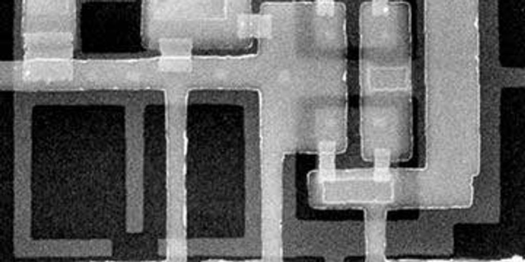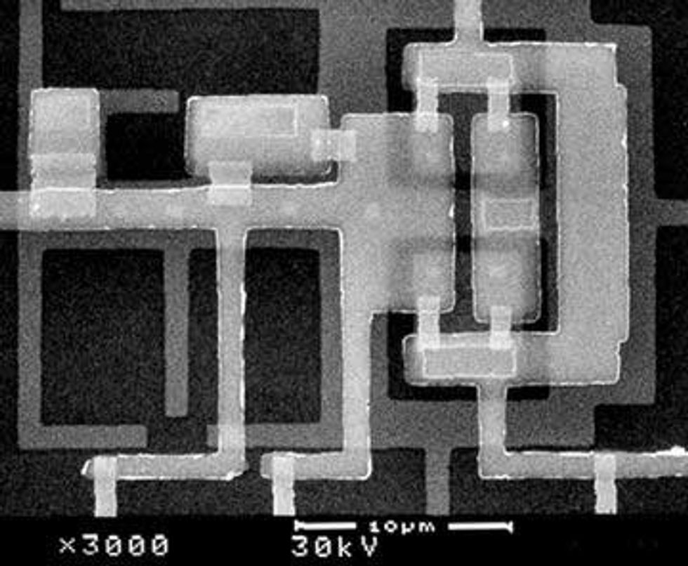
IMAGE: JAMES LUKENS, STATE UNIVERSITY OF NEW YORK AT STONY BROOK
[1] Researchers have demonstrated simple digital frequency dividers with Josephson junctions that have 0.25-µm minimum features and that operate at data rates up to 770 Gb/s. They rely on rapid single flux quantum (RSFQ) circuits, whose speed grows as junction sizes shrink. At 0.25 µm, the junctions are intrinsically nonhysteretic, a good sign for the future of complex chips operating at clock frequencies of 100 GHz.
The fastest integrated circuits in the world today are unique for their technology as well as for their speed. They are made with a superconducting metal, niobium, rather than a compound semiconductor. Their exotic technology is based on Josephson junction devices and the transmission of single quanta of magnetic flux along superconductor interconnects.
Except that they, too, operate at temperatures below 10 K, these superconductor ICs are quite different from those studied through the early 1980s in U.S. industrial laboratories. By chance, about the time those programs shut down, a number of discoveries nurtured a radically revised second generation of materials and circuit fabrication processes. A new logic family was also developed that promised huge improvements in circuit speed. Called rapid single flux quantum (RSFQ) logic, it is based on the storage and transmission of quanta of magnetic flux [see “The origins of magnetic flux quantum devices“].
Now that problems plaguing low-temperature superconductor electronics have been solved, commercial viability is at last on the way. And performance is spectacular. RSFQ logic can operate in complex circuits at clock frequencies beyond 100 GHz. The technology is also rugged. Fabricated with a new process that produces more reliable Josephson junctions, and building on other developments, RSFQ circuits are at the heart of commercial systems that could be available within five years [see ” Fabricating the novel Josephson junctions“].
The first RSFQ products will probably leverage superconductor superiority in performing high-speed and high-accuracy analog-to-digital conversion. Given adequate resources, the next few years are likely to see the first superconductor digital RF modules for both wireless communications base stations and high-performance instrumentation. Other potential applications include petaflops computing platforms and high-throughput and high-density network switches. In short, thanks to two key features–speed conjoined to low power and analog-to-digital quantum accuracy–RSFQ circuits should extend digital power and flexibility directly into the RF and microwave domains.
Such applications are now practical because the linewidths of Josephson junction devices are shrinking to about 1 µm–down from 2-3 µm–pushing the performance of these very large-scale integration (VLSI) ICs well past anything their semiconductor counterparts can do. Meanwhile, the development of powerful, small, closed-cycle refrigerators makes it practical to integrate room temperature semiconductor systems with cryogenic superconductor systems. Hybrid systems of this kind will allow RSFQ to undertake the fastest tasks, with semiconductors (possibly chilled) performing functions that need large-scale integration, lower speed, and the interface to room temperature.
Dazzling talents
The second-generation technology has striking attributes. First, its performance is scalable. There are no known physical barriers to decreasing size by a factor of 10 and thus increasing speed by a factor of 10, using lithography to move from today’s 3-µm linewidth to 0.3 µm. Work is ongoing at the State University of New York (SUNY) at Stony Brook, to explore how far it can get by scaling simple gates to the 0.25-µm linewidths of today’s semiconductor processes. In fact, data rates of more than 750 Gb/s have already been experimentally demonstrated for RSFQ toggle flip-flops having gates of this size [Fig. 1].
Accuracy at such blinding speeds is another built-in feature of Josephson junctions. The ac Josephson effect allows the frequency of output bits (fluxons) to be inferred from a simple measurement of voltage, where each microvolt corresponds to a data rate of 483.5 Mb/s. In fact, this correspondence has been certified to 3 parts per billion by the U.S. National Institute of Standards and Technology (NIST), in Boulder, Colo. So accurate is this technique that it was adopted in 1990 as the official Système Internationale (SI) definition of the volt in standards laboratories around the world. Digital RSFQ circuits in 1.5-µm and 0.8-µm processes have been tested at Hypres with the unambiguous results that the measured voltage is indeed a product of digital operations, and that the output data rate scales as expected–doubling with each halving of linewidth and appropriate adjustment of other circuit elements. Further support comes from theoretical studies in the United States and abroad that match well with the experimental data.
Next there’s circuit density. Because Josephson devices and their superconducting interconnects dissipate hardly any power, they can be very densely packed without overheating. For instance, RSFQ circuits made with minimum Josephson junctions 0.3 µm on a side and running at clock frequencies of 250 GHz could pack individual devices as close as 1 µm, herding some 100 000 devices onto a 0.5-cm2 chip dissipating less than 0.25 W.
More important still, signals propagate virtually without dispersion. This fact, plus the pipelined architecture made possible by superconducting passive and active interconnects, removes a key obstacle to semiconductor circuits increasing clock speeds by scaling: the significant delay associated with on-chip interconnects, as identified in the 2000 Semiconductor Industry Association’s International Technology Roadmap for Semiconductors.
A state of flux
The Josephson effect was predicted by Brian Josephson while a student at Cambridge University, in England, in 1962, and the first devices were made by Philip Anderson and John M. Rowell at Bell Laboratories, in Murray Hill, N.J., in 1963. A modern Josephson device comprises an insulating layer sandwiched between two superconducting films–the insulation being so thin that electrons can tunnel through it in pairs. These pairs of electrons, or Cooper pairs, also carry current in superconductors. (Leon Cooper, along with John Bardeen and Robert Schrieffer, won the 1972 Nobel Prize in Physics for the development of the BCS theory of superconductivity.) The insulating barriers are often called weak links because the electron pair current through them is 1/1000 to 1/10 000 the size of the maximum pair current that can be carried in the superconductor electrodes. Whereas in silicon FETs, tunneling through the gate oxide is undesirable, in Josephson junctions the tunneling current is essential.
From the mid-’60s to the mid-’80s, superconductor digital ICs relied on logic schemes in which Josephson junctions with hysteretic I-V curves were switched from the superconducting (0) state to the resistive (1) state. In today’s RSFQ technology, the junctions are shunted externally with a resistor, so that the I-V characteristic is nonhysteretic. This allows circuit designers to exploit another superconductivity phenomenon–the macroscopic quantization of magnetic flux.
In RSFQ circuits, it is not a static voltage level, but the presence or absence of quantized magnetic flux (fluxons) that represents information bits. The basic RSFQ structure is a superconducting ring that contains one Josephson junction plus a resistive shunt outside it [Fig. 2]. Suppose a current is already circulating around the loop, supporting one fluxon. At a certain critical current level (about 100 µA for typical designs), additional dc current across the loop causes the quantum of flux to be ejected, with the Josephson junction acting as a briefly opened exit ramp.
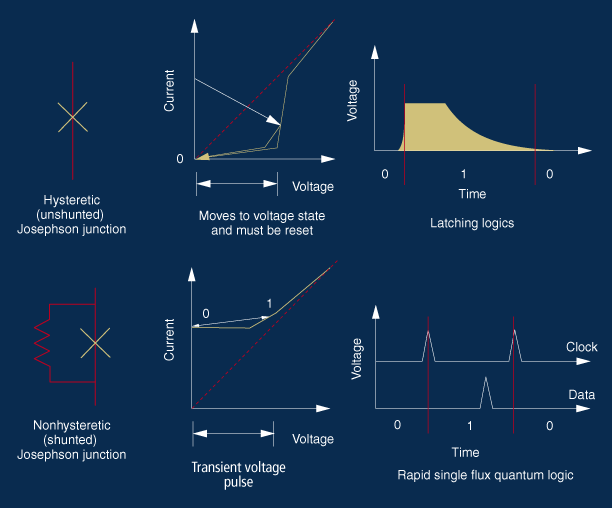
[2] Through the mid-’80s, superconducting digital ICs relied on logic schemes in which Josephson junctions [top left] switch from electron-pair tunneling current at zero voltage to a resistive state of single-electron tunneling [top center]. The device remains latched in the voltage state until the current returns to zero [top right].
RSFQ devices are much faster because the junctions are shunted externally with a resistor [bottom left], resulting in I-V characteristics that are nonhysteretic [bottom center]. Logic functions are built around the voltage pulses that occur each time a flux quantum enters or leaves the superconducting loop.
Click on image to enlarge.
Rather than use the escaping flux directly, RSFQ relies on the fact that the movement of a fluxon into or out of this loop induces a very short voltage pulse across the junction. If the Josephson junction were a square, 1 µm on a side, this voltage pulse would be about 1 ps long and 2 mV in amplitude. The SFQ pulses become briefer and taller as the junctions dwindle in size, but the voltage-time product of the pulse (which is equal to the quantum of magnetic flux passing through the junction) always remains the same: 2mV-ps, which is equal to 2 x10-15 weber. The energy consumed each time an SFQ pulse passes through a junction is just the circulating current of about 100 µA times the amount of flux *0 or about 2 x 10-19 joule, a very small figure indeed!
The voltage pulses can be transmitted ballistically to other gates over either microstrip transmission lines or active Josephson transmission lines, the latter so-called because they contain extra Josephson junctions as repeaters of the pulse, providing delays for timing synchronization. Naturally, all interconnects are superconducting and therefore lossless, at least at dc, and the losses remain low, compared to metals at room temperature, up to clock frequencies of about 750 GHz.
To transfer the pulses as bits of information, a clock provides a steady stream of timing pulses (one for each clock cycle), such that the presence of a data pulse within the clock cycle denotes a logic 1, while the absence of the pulse denotes a logic 0. Combinations of Josephson junctions can then be interconnected to achieve SFQ pulse fan-in and fan-out and create a variety of logic structures. Although all common binary logic primitives (like AND, OR, or XOR) can be fashioned, it is often more convenient to create gate macros directly rather than from lower logic primitives. This technique maximizes speed and minimizes junction count.
All RSFQ circuits are composed of three basic building blocks [Fig. 3]. The blocks provide all necessary circuit dynamics: transferring SFQ pulses from one device to another, storing SFQ pulses, and making the binary decision whether or not to transmit a pulse. Any binary function can be constructed from these elements. A bonus is that such logic is inherently micro-pipelined, due to the natural memory at the gate level, and excellent at controlling clock skew in high-frequency circuits.
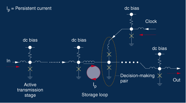
[3] Any binary function can be constructed from three types of RSFQ building blocks. The transfer block, a Josephson junction [indicated by an X] plus a 6-pH inductor [left], moves pulses from one device to another. The storage loop, a junction and an inductor of about 12 pH, stores pulses in a persistent current loop, Ip [middle]. The decision-making pair, which consists of junctions of two different sizes [right], determines whether or not to send a pulse to the next device.
Click on image to enlarge.
The operation of an RSFQ reset-set flip flop gate is a simple example [Fig. 4]. If a set pulse arrives, J1 transmits it into the quantizing inductance loop, where it becomes trapped as a circulating current–the 1 state. This current biases J3, so that when a clock/reset pulse arrives at the gate, it causes J3 to transmit the stored fluxon to the output, thus resetting the flip-flop to the 0 state. Alternatively, if no set pulse input has occurred during the clock period and a clock/reset pulse arrives, the unbiased J3 cannot transmit the pulse and J2 is forced to let the fluxon escape the circuit. Result: no pulse at the output.
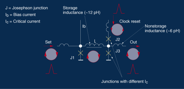
[4] Like a semiconductor flip-flop, an RSFQ reset/set flip-flop gate can assume one of two stable states. It uses all three RSFQ building blocks: the transmission stage [leftmost inductor and junction J1], the storage loop [center] and the decision-making pair [to right of storage loop].
When a set pulse arrives, Josephson junction J1 transmits it into the storage loop, where it is trapped as a circulating current–the logic 1 state. This current biases J3, the bottom junction of the decision-making pair, so that the arrival of a clock/reset pulse causes J3 to transmit the stored flux quantum, or fluxon, to the output, resetting the flip-flop to the logic 0 state.
If no set pulse occurs during the clock period and a clock/reset pulse arrives at the decision-making pair, J3 cannot transmit the pulse and J2 must let the fluxon escape the circuit, resulting in no pulse at the output.
Click on image to enlarge.
All RSFQ cells use this method of local gate memory setting a biased decision-making pair. The entire transaction takes from less than 1 ps to a few picoseconds, depending on the size of the Josephson junctions. It also consumes merely 1 µW or so, nearly all of which comes not from the junction device but from the gate’s on-chip bias resistors, which draw a few hundred microamperes from a 2-mV supply.
A primary contribution of the RSFQ approach to performing logic with SFQ pulses was a neat convention for the logical representation of 1s and 0s. This convention made RSFQ a synchronous (clocked) logic at the gate level, departing from the combinatorial, asynchronous, boolean gates of mainstream semiconductor logic. Since the mid-’80s, other logic families utilizing flux quanta have been proposed; nevertheless, the RSFQ convention for performing digital and mixed-signal logic with superconductors is now preferred by most researchers around the world.
Circuits and packages
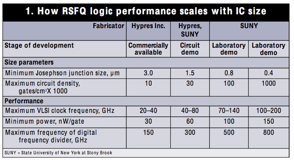
RSFQ chip performance over three generations of low-temperature superconductor technology has been projected by Konstantin Likharev (at SUNY Stony Brook) and is supported by experimental data. Likharev concludes that RSFQ speed and packing density will keep increasing as Josephson junctions scale down to about 0.4 µm [Table 1], conservatively yielding VLSI clock frequencies of over 100 GHz.
To move the RSFQ field toward commercialization, engineers have been developing a practical infrastructure of circuits and techniques. They have demonstrated on-chip digital clocks and phase-locked loops; analog-to-digital and digital-to-analog converters; first-in, first-out memory buffers and random-access memories; adders and multipliers; multiplexers and demultiplexers; network switching fabrics; digital autocorrelators; digital output amplifiers; and more.
Nor have gigahertz-speed cryopackaging, direct optical I/O, and semiconductor interface electronics been overlooked. The cryopackage cools the chip to its low operating temperature, supplying it with power and making I/O connections. Obviously, the power and signal connections must not warm the chip beyond its operating temperature. Ribbon cables with very thin copper traces to limit heat input have been developed by Tektronix Inc., Beaverton, Ore., IBM Corp.’s Thomas J. Watson Research Center, Yorktown Heights, N.Y., and others, under a program managed by the U.S. National Security Agency, Fort Meade, Md. The superconductor chips themselves are cooled on the cold head of a closed-cycle refrigerator; the power and I/O leads are cooled by the refrigerator before they reach the chips.
An attractive way of introducing signals into the chip is over an optical fiber, because it transmits almost no heat between the chip and the system it serves. Optical fibers are also the only interconnect medium that can match the highest data rates possible with RSFQ logic–well above 100 Gb/s. At the University of Rochester, in New York, metal-semiconductor-metal diodes created on the silicon substrates of RSFQ chips have been used to convert laser-modulated data signals directly into fluxons in RSFQ circuits for processing. Because the energies of SFQ pulses are tiny, direct outputs from the circuits must be amplified before driving the output laser or modulator. Conductus Inc., Sunnyvale, Calif., has had success in demonstrating the full path of optical I/O at multigigahertz speeds.
To transmit signals between RSFQ chips, superconducting multichip modules have also been developed, particularly at TRW Inc., in Redondo Beach, Calif., where superconductor chips are flip-chipped and bump-bonded, as in semiconductor packages. Because the interconnects and the multichip module are superconducting, signal propagation is ballistic and free of dispersion. Generally, even with these ideal modules, the RSFQ signal pulses need superconducting digital amplifiers on chip, to guarantee their propagation through the bump bonds. Recently, though, direct transmission of the RSFQ pulses onto a multichip module was achieved, an indication that eventually the on-chip amplifiers may be unnecessary.
The killer apps
Ultrahigh-performance analog-to-digital (A/D) converters are key to bridging the RF and digital domains. System designers will be able to circumvent the cost, redundancy, and inflexibility of dedicated analog RF subsystems once microwave signals are directly digitized with a technology that can process the data stream at speed. Direct digitization of RF signals has been achieved by an RSFQ high-resolution A/D converter based on a phase-modulation/demodulation architecture being developed at Hypres [Fig. 5]. This architecture, coupled with the quantum accuracy bestowed by superconductors on A/D discrimination levels, enables the performance required for direct digitization of such signals. Even at the current state of maturity, this superconductor A/D converter outperforms any reported technology.
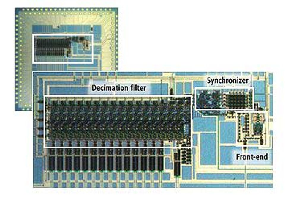
[5] RSFQ-based analog-to-digital converters exploit the natural phenomenon of magnetic flux quantization to provide extremely linear and high-speed digitization of analog signals. This 1-cm
2 chip, fabricated in a 3-µm technology, contains over 2500 Josephson junctions, and runs at a clock frequency of 12.8 GHz.
Click on image to enlarge.
Furthermore, while conventional semiconductor-based A/D developers fight to squeeze in additional performance, despite reaching fundamental limitations of lithography and component matching, superconductor A/D converters are just beginning to exploit their fabrication process. They also stand to scale up their performance as the designs are taken from the present 2-3-µm process into the emerging 1-µm niobium VLSI fabrication processes.
The Hypres A/D converter consists of three major parts: a differential-code analog phase modulator (front end), a digital phase-demodulating time-interleaved bank of race arbiters (synchronizer), and a digital decimation low-pass filter. The 1-cm2 die [Fig. 5] has over 2500 Josephson junctions and runs at a clock frequency of 12.8 GHz.
A singular feature of this design, and one of tremendous value in broadband systems, is that it is dynamically programmable: it allows the user to trade off bits for bandwidth in real time. (Semiconductor A/D converters, in contrast, are rarely designed for more than one operating frequency.)
Utilizing flux quantization in superconductors, this A/D converter calls directly on the ratio of fundamental constants (h/2e) that define the flux quantum, so as to set the linearly spaced quantization thresholds needed for digitization with quantum mechanical accuracy. The ultralinear nature of the converter’s front end means that high sampling rates in the multigigahertz range can be combined subsequently with time-averaging to extract more accuracy without adding nonlinearities to the conversion. No other technology has this feature, either.
Interest in such designs remains high among wide-band communications and radar systems designers, partly because of likely dual-use applications in civilian markets, such as all-digital software-defined radio for wireless communications. In communications applications, the superconductor circuits and systems would be located in existing base stations, which can easily accommodate rack-mounted packages. With the superior receiver sensitivity and accuracy, this configuration can relieve some of the requirements on the handsets and terminals. Hypres and Northrop Grumman in Baltimore, Md., are both also working on superconductor D/A converters for improved linearity and speed on the transmit side.
Because of the compatibility with fiber optics, a number of research projects in superconductor communications switches have been completed or are ongoing. One Advanced Technology Project (ATP) was a joint venture of the U.S. Department of Commerce, Conductus, TRW, the University of California at Berkeley, and Stanford University, in collaboration with the National Institute of Standards and Technology, and Hypres. They built a hybrid system that contained RSFQ chips on a superconducting multichip module operating at 5 K, interfaced to semiconductor components operating at 80 K and at room temperature. Digital signals at 8 Gb/s were transmitted on optical-fiber interconnects to the superconductor switch, which was packaged with a cryocooler, or cryogenic refrigerator.
RSFQ switch projects are also under way at Hitachi and NEC, funded by Japan’s International Superconductivity Technology Center (Istec). There is also a collaborative effort between TRW and Irvine Sensors.
Advantages AND disadvantages
Fabricated with the Hypres 3-µm niobium IC technology, T flip-flops have run at clock frequencies over 120 GHz, and complex FIR filters, flash A/D converters,and other digital logic at up to 20 GHz. Moreover, unlike other emerging high-performance technologies, such as indium phosphide heterojunction bipolar transistors or resonant tunneling diode schemes, RSFQ circuit power dissipation hardly scales at all with operating frequency. Not to be forgotten is the operating temperature of the superconductor IC itself. The deep chill reduces thermal noise to 1-2 percent of that in room-temperature circuits, so that error rates in digital circuits are very low. Also, unlike other proposed multigigahertz technologies, Josephson junction ICs are already at integration scales of up to 10 000 or 20 000 devices per chip.
One special advantage of RSFQ logic is that its high speed coincides with low power. It is projected that within two lithography generations, leading from the current 2- to 3-µm minimum features down to 0.8 µm, clock frequencies of 100 GHz will occur at power levels per gate that are about 100 000 times lower than in silicon. (Of course, advanced layout and computer-aided design techniques will have to be adopted as well.) The achievement could take as little as a couple of years if the proper investments are made. This speed-at-low-power advantage matters most for chips of the highest integration levels.
Nor are expensive fabrication facilities needed. Photolithography that is almost obsolete for silicon–about 1 µm for critical dimensions–will do, so that second-hand equipment can be used. RSFQ fabrication itself is much simpler than for any semiconductor, since no wafer-heating steps (involving epitaxial growth, doping drive-ins, or ion implantation) are used.
Only simple refractory films and insulators are sputtered onto a silicon wafer, which can remain close to room temperature. It is perhaps this simplicity of the process that has allowed so much progress to be made by a few small research groups. Interestingly, the lack of investment in fabrication facilities is what mainly limits the integration density of manufacturable superconductor ICs.
Also, because RSFQ ICs rely on an all-thin-film fabrication process, they are intrinsically radiation-hardened–about 50 times more tolerant than hardened semiconductor chips. The SFQ pulses travel at almost the speed of light and suffer negligible attenuation, dispersion, and crosstalk, the bane of interconnects in semiconductor counterparts.
Like all good things, these intrinsic advantages come at a price–in this case, the cost of cryogenic cooling plus the need for more complex packaging and more difficult testing. Further, advances must be made in delivering the performance from the cold chip to the user at room temperature.
The technology has other disadvantages as well. No gain is produced in Josephson junctions, so fan-out is more cumbersome than with transistors. Because Josephson junctions are low-power devices, special circuits have to be fashioned to interface with the somewhat larger static voltage logic levels of, say, emitter-coupled logic. Because single quanta of flux serve as data, it is essential not to trap any unwanted flux in the chip during cooling. This adds to design and packaging constraints.
Progress was made in addressing these issues in the early days of the technology at IBM, and more recently at SUNY, Hypres, and the University of California at Berkeley. The techniques involve packaging designs that effectively reduce the magnetic field in the vicinity of the IC, as well as special layout techniques in which ground plane holes, known as moats, trap stray magnetic flux in regions away from the active part of the circuit. As the number of Josephson junctions per chip rises past about 100 000, new bias resistor schemes may also be needed to minimize the total current through any one I/O channel in the package.
Steps to commercial feasibility
To say the least, commercializing a technology like RSFQ will be full of challenges. Some will be common to all technologies attempting to enter the unexplored realm of high-frequency and high-integration-density operation, and others will be specific to superconductors.
At speeds up to 100 times those of fast semiconductor ICs, all technologies will have to grapple with the distributed nature of the electromagnetic signals, the inadequacy of computer-aided design tools, and the generation and distribution of a clock signal on chip and between multichip modules. As no test instruments yet exist for ICs of these frequencies, built-in self-test will be indispensable. Interconnect delays, both on and off chip, will also limit the performance of any technology that uses interconnects at or above room temperature.
Issues specific to RSFQ circuits at these frequencies include: obtaining the investment needed to advance commercially available technology to the submicron regime; achieving good enough yields; testing at temperatures near absolute zero; and developing reliable compact “invisible” cryocoolers and packages that will deliver the RSFQ speed advantage to the customer.
Encouragingly, advances have also been made recently in the technology of cryocoolers, which cool niobium superconductors to their best operating temperature of about 5 K. While liquid helium (at 4.2 K) is usually used for testing in research laboratories, cryocoolers that require no liquid cryogens and run virtually unattended for years on end are preferable for commercial or military products. Over the past decade, their reliability and efficiency have improved, while their size and cost have declined.
These days, about US $20 000 can buy a cryocooler that reaches down to 4-5 K and fits in the lower half of a standard 48-cm instrument rack. Commercial systems using off-the-shelf cryocoolers are now obtainable from Hypres to realize the SI definition of the volt; they require routine maintenance only once every 24 months. Further reductions in size, cost, and increased efficiency of cryocoolers should stem from increased volume of production and the availability of a cooler developed with cryogenic electronics as its specific application.
Coming in from the cold
Ironically, it may be the psychological obstacle of using a cryogenic technology, rather than a technical one, that RSFQ designers will have to overcome before seeing these second-generation superconductor ICs reach systems in the field. But success here is sure to lead to rewards in higher-performance systems and in leveraging a technology that is at the dawn of its career. Simultaneously, action here may expand the capabilities of established semiconductor technologies, whose sun may be starting to set as they near their physical and economic limits. The drivers for marrying the two technologies will be the market’s demand for higher bandwidth and for seamless RF and digital integration. The catalysts for translating these demands into market realities will no doubt include visionary investors, determined engineers, and creative environments.
About the Authors
Darren K. Brock (M) and his coauthors are associated with Hypres Inc. of Elmsford, N.Y., a commercial design house and foundry for superconductor ICs. Brock is director of advanced development there and has been designing rapid single flux quantum ICs using the Hypres fabrication process since 1992.
Elie K. Track (M) is consulting partner and member of the Hypres Scientific Advisory Board, and a former president and chief executive officer. Active in the field of superconductivity since 1982, he is also a member of the Executive Board of the Yale Science and Engineering Association.
John M. Rowell is chairman of the Hypres Scientific Advisory Board, and is the Materials Institute Professor at Northwestern University, in Evanston, Ill. He was the first to observe the Josephson effect in 1963, and is a co-inventor of the modern niobium/aluminum trilayer fabrication process. He was previously at Bell Laboratories, Bell Communications Research, and Conductus. He is a member of the National Academy of Science and the National Academy of Engineering, and is a Fellow of the Royal Society.
To Probe Further
Josephson latching logic is covered in “The Superconducting Computer,” by J. Matisoo, Scientific American, May 1980, pp. 50-65 and “Computing at 4 degrees Kelvin,” by W. Anacker, IEEE Spectrum, May, 1979, pp. 26-37, and “Superconducting Electronics,” by D. McDonald, Physics Today, February, 1981, pp. 36-47.
Rapid single flux quantum (RSFQ) logic is covered in K. Likharev’s “Superconductors speed up computation,” Physics World, May 1997, pp. 39-43.
An excellent source of references to applied superconductivity, compiled by Terry Orlando at the Massachusetts Institute of Technology, can be found on the Web at the following address: http://web.mit.edu/6.763/www/FT99/refmat/refmat.html.
A comprehensive technical review of “RFSQ Technology: Physics, Devices, Circuits, and Systems” will be published in a special issue on 100-GHz logic of the International Journal of High Speed Electronics and Systems, January 2001 (the issue’s guest editor is M. Rodwell). The article’s authors are P. Bunyk, K. Likharev, D. Zinoviev, and D. Brock.
