By Greg Curtis and YuLing Lin
Innovation is everywhere around us. From high-performance computing, communications, autonomous driving, and the Internet of Things (figure 1), each segment has led to a rapid increase in design innovation. This innovation has been particularly true in communications, as Radio Frequency (RF) technology is found everywhere in daily life. RF technology is critical to many aspects of modern electronics as it is incorporated into almost everything that transmits or receives a radio wave across the entire RF spectrum (3 KHz to 300 GHz), including mobile phones, radios, Bluetooth, Wi-Fi and 5G applications. In order to properly verify these designs before silicon fabrication, specialized RF analyses are required incorporating a time domain method, Shooting Newton (SN), and a frequency domain method, Harmonic Balance (HB), to accurately predict silicon behavior.

Fig. 1: Analog, RF, and Mixed-Signal Applications
Nanometer circuit RF verification challenges
While there are many benefits to migrating to smaller process geometries, such as lower power and higher performance, RF designers using nanometer CMOS technology must battle with the growing design complexity, such as decreasing voltage levels, leading to concerns for circuit nonlinearity and device noise impact.
A contributing factor to design complexity is the significant increase in resistance and capacitance parasitics. Because of this, simply simulating the schematic design without the inclusion of the layout effects introduces a huge risk, as it no longer represents an accurate analog model of the design, which results in the growing challenge of post-layout simulation.
These design complexities require designers to adopt digital calibration and compensation techniques and to incorporate layout from the initial design phase to optimize for performance and power consumption. Therefore, a comprehensive verification plan is required encompassing process mismatch, voltage, and temperature variations, as well as inclusion of layout effect and RF analyses for sweeping of power, frequency, and bit tuning, for the final design signoff before tape-out.
In order to overcome the design and verification challenges for RF circuit design, two analysis methods have emerged for modern RF simulator engines to verify circuits for linearity, noise, and gain. One is based in the time domain (Shooting-Newton) and the other based in the frequency domain (Harmonic Balance). Each method is optimal for specific targeted applications. The Shooting-Newton approach is applicable to all periodic circuits, particularly circuits with sharp transitions. The Harmonic Balance approach is most applicable for circuits which exhibit linear to moderately nonlinear distortion, require high numerical dynamic range, and use frequency domain models such as tabulated S-parameters.
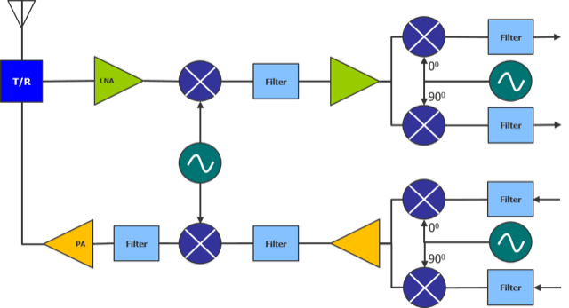
Multi-tone simulations are typical when designing modern-day transceivers (figure 2), where two or more periodic signals at unrelated tone frequencies are the stimuli applied to the circuits. These simulations are challenging to handle in the time domain due to narrow tone spacing and very time consuming since the minimum time step must be compatible with the highest frequency. Harmonic Balance analysis makes it feasible and practical to simulate circuits with multiple input frequencies. When the frequency spectrum is sparse, multi-tone harmonic balance simulations are faster, require less memory, and have improved accuracy, compared to time-domain approaches. Multi-tone simulation runtime can be impacted by several factors, such as circuit size and the number of tones. As an example, moving from a single-tone simulation to a three-tone simulation to accurately determine the impact of intermodulation distortion such as the 2nd and 3rd order IM products (IM2 and IM3), designers must increase the number of intermodulation terms to ensure accuracy which can result in an increased simulation time of 9x, and in some cases make the post-layout version of the design only practical when using the most advanced simulation engines with the latest advances in multi-threaded solvers and model evaluation. This is especially true for finFET designs at the most advanced nodes.

Fig. 2: Modern-day Transceiver
Nanometer circuit RF verification platform
Analog FastSPICE (AFS) offers a Shooting Newton as well as a Harmonic Balance engine for both single-tone and multi-tone HB, Noise (HBNOISE), AC (HBAC), Stability (HBSTB), Scattering Parameter (HBSP) and Transfer Function (HBXF) analyses. For superior accuracy and performance on linear and near-linear circuits, the AFS harmonic balance solvers are further optimized for performance and convergence via automated intelligence algorithms, with no compromise in accuracy.
AFS harmonic balance analyses are available as part of the Analog FastSPICE Platform at no additional cost to existing customers. The AFS Platform is foundry-certified accurate by the world’s leading foundries, delivering nanometer SPICE accuracy >5x faster than traditional SPICE and >2x faster than parallel SPICE simulators. With the recently announced Analog FastSPICE eXTreme technology for nanometer-scale verification of large, post-layout designs, an additional performance boost of up to 10X is possible as compared to the previous generation.
The AFS Platform delivers over 50M-element capacity and the fastest mixed-signal simulation with Symphony. For silicon-accurate characterization, the AFS Platform includes the industry’s only comprehensive full-spectrum device noise analysis and integrates with Solido Variation Designer delivering full variation-aware design coverage in orders-of-magnitude fewer simulations, but with the accuracy of brute force techniques.
Nanometer RF circuit design requires extensive sweeps, corners, and Monte Carlo analysis. AFS HB utilizes multi-threaded capability for an additional performance speedup versus single core operations. The AFS Platform is integrated with Solido Variation Designer to address comprehensive corner variation results efficiently. It allows a more effective verification providing accuracy with less number of simulation across all environmental corners, reducing the RF simulation complexity.
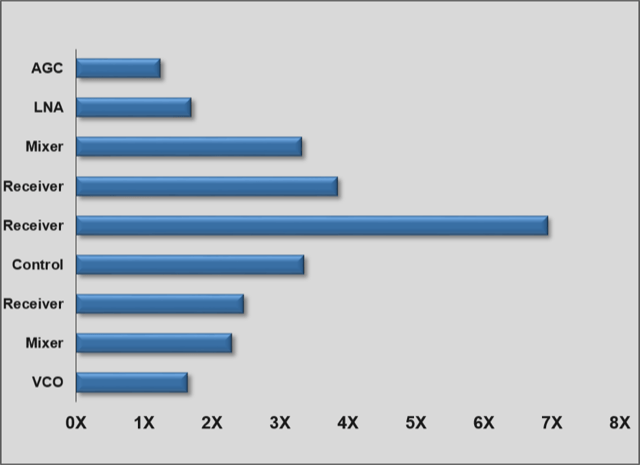
In recent benchmarks comparing critical RF metrics such as second and third order intercept (IP2 and IP3), 1dB compression point (P1dB), AFS HB was able to meet the stringent accuracy requirements and provide a simulation performance improvement as compared to other commercially available solutions at similar accuracy settings on process nodes from 65nm down to 7nm process nodes. AFS HB showed an average speedup of 2.6x faster for post-layout designs (Figure 3) and 1.8x faster for pre-layout designs. For some of the most challenging post-layout multiple tone simulations, AFS HB was the only solution to converge and provide accurate results.

Fig. 3: AFS HB Simulation Speedup
Summary
With the increasing complexities of high performance computing, communications, autonomous driving, and the Internet of Things, design innovation is increasing at an even faster rate. This has been particularly true in communications as Radio Frequency (RF) technology is found everywhere. RF technology is critical to many aspects of modern electronics. In order to properly verify these designs prior to silicon, specialized RF analyses are required to accurately predict silicon behavior.
For challenging nanometer analog, RF, and mixed-signal circuit verification, the Analog FastSPICE platform delivers the most accurate, comprehensive, and highest-performance verification capabilities available in a single-executable platform and is foundry certified accurate by the world’s leading foundries at the most advanced process geometries, addressing RF technology that is found everywhere in daily life.
YuLing Lin is a solutions architect at Mentor, a Siemens business.

