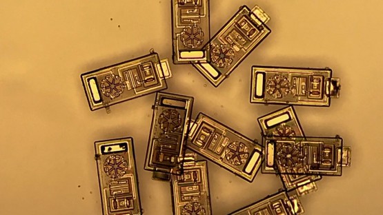
Theologians once pondered how many angels could dance on the head of a pin. Not to be outdone, Cornell researchers who build nanoscale electronics have developed microsensors so tiny, they can fit 30,000 on one side of a penny.
There’s more to these tiny sensors than just their diminutive size: They are equipped with an integrated circuit, solar cells and light-emitting diodes (LEDs) that enable them to harness light for power and communication. And because they are mass fabricated, with up to 1 million sitting on an 8-inch wafer, each device costs a fraction of that same penny.
The team’s paper, “Microscopic Sensors Using Optical Wireless Integrated Circuits,” published April 17 in PNAS.
The collaboration is led by Paul McEuen, the John A. Newman Professor of Physical Science, and Alyosha Molnar, associate professor of electrical and computer engineering. Working with the paper’s lead author, Alejandro Cortese, Ph.D. ’19, a Cornell Presidential Postdoctoral Fellow, they devised a platform for parallel production of their optical wireless integrated circuits (OWICs) – microsensors the size of 100 microns (a micron is one-millionth of a meter), mere specks to the human eye.
“In a certain sense, it’s an old idea, building tiny sensors like this,” said McEuen, who co-chairs the Nanoscale Science and Microsystems Engineering (NEXT Nano) Task Force, part of Cornell’s Radical Collaboration initiative. “But we pushed it another order of magnitude down in size and made it mass fabricate-able. A lot of times when people would make these little doodads, they would wire them all together by hand. You didn’t get a million at a time. So we constrained ourselves and said we’re not going to do it unless we can make them by the million.”
The OWICS are essentially paramecium-size smartphones that can be specialized with apps. But rather than rely on cumbersome radio frequency technology, as cellphones do, the researchers looked to light as a potential power source and communication medium.
Placing tiny circuits on a silicon wafer is relatively easy in the nanotech arena, McEuen said, but adding LEDs is a special challenge because they are made with a different material: gallium arsenide. In order to transfer the LEDs to a wafer with the electrical components and integrate them, the researchers developed a complicated assembly method that involved more than 15 layers of photolithography, 30 different materials and more than 100 steps.
“There are a lot of people working at larger scales where you can pick up things and see them with your eye and touch them. This is not that,” Cortese said. “It’s at a scale that you legitimately cannot see what you’re doing unless you’re under a microscope. So you really have to gain an intuition about the nanoscale and the microscale.”
Once the OWICs are freed from their substrate of silicon, they can be used to measure inputs like voltage and temperature in hard-to-reach environments, such as inside living tissue and microfluidic systems. For example, an OWIC rigged with a neural sensor would be able to noninvasively record nerve signals in the body and transmit its findings by blinking a coded signal via the LED.
As a proof of concept, the team worked with the lab of Chris Xu, professor of applied and engineering physics and a co-author of the paper, and successfully embedded an OWIC with a temperature sensor in brain tissue and wirelessly relayed the results.
McEuen, Molnar and Cortese have launched their own company, OWiC Technologies, to commercialize the microsensors. A patent application has been filed through the Center for Technology Licensing. The first application is the creation of e-tags that can be attached to products to help identify them.
The tiny, low-cost OWICs could potentially spawn generations of microsensors that use less power while tracking more complicated phenomena.
“The circuits in this paper were quite simple,” Cortese said. “But you can potentially fit thousands of transistors on one of these devices. And that means you can increase the range of things the device can sense, how the device communicates out, or it’s ability to complete more complex tasks. We really developed this as a platform so that a lot of people have space to develop new devices, new applications.”
Molnar and Xu are members of the Kavli Institute at Cornell for Nanoscale Science, which McEuen directs.
Contributing authors include doctoral students Conrad Smart, Michael Reynolds, Samantha Norris, Yanxin Ji, Fei Xia, Aaron Mok and Chunyan Wu; postdoctoral researchers Sunwoo Lee and Tianyu Wang; and Nathan Ellis, machine shop manager of the Laboratory of Atomic and Solid State Physics. The researchers developed their fabrication process with the assistance of the Cornell NanoScale Science and Technology Facility.
The research was supported by the Cornell Center for Materials Research, with funding from the National Science Foundation’s Materials Research Science and Engineering Center program, the Air Force Office of Scientific Research and the Kavli Institute. Additional funding was provided by the National Institutes of Health and the National Science Foundation Graduate Research Fellowship.


