Introduction
Contents
With recent advancements in process technology, such as the development of high resistivity substrates, the integration of passive devices on-die, and the integration of bipolar junction transistors (BJTs) and complementary metal-oxide-semiconductor (CMOS) technologies into a new BiCMOS technology, combined with general technology scaling, the integration of RF components has evolved from a purely discrete component solution space to more compact, low power IC solutions that provide good noise figures (NF) and linearity for a wide range of frequencies.
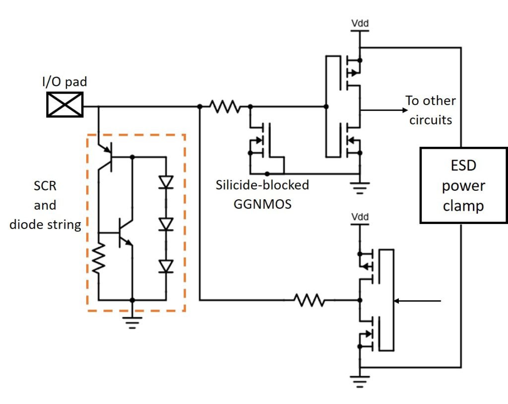
This evolution also amplified the trend toward system-on-chip (SoC) designs, where the RF front end exists on the same IC as the digital baseband processor and memory modules (Figure 1) [1]. It is now common to see auxiliary circuit blocks, such as analog to digital converters (ADCs), digital to analog to digital converters (DACs), phase-locked loops (PLLs), frequency synthesizers, voltage references, and biasing circuits (e.g., bandgaps and current mirrors), on the same die as the RF front-end blocks. While expanding baseband integration significantly improves performance and efficiency, the added complexity creates increased verification challenges for these RF ICs.
Figure 1. Conceptual block diagram of typical modules found in modern RF SoCs.
Let’s take a closer look at the types of checking that can be used on these designs to find and eliminate these impacts on reliability and performance, and how advanced electronic design automation (EDA) tools and techniques are helping designers ensure accurate, fast, automated verification and design for manufacturing optimization of RF ICs.
RF IC verification challenges
For a given process, foundries typically offer various device types and device variants for components such as diodes, resistors, capacitors, field-effect transistors (FETs), BJTs, etc. These
device types or variants have different characteristics, such as threshold voltage (Vt), breakdown voltages and currents, thermal resistances, noise figures, allowable device dimensions, etc. [3]. Depending on the device characteristics and foundry design rules, it is desirable (and in some cases, mandatory) to use specific devices in specific circuits.
For example, metal-oxide-semiconductor field effect transistors (MOSFETs) are frequently used in RF ICs for their performance characteristics. While it is generally desirable to use shorter channel lengths for circuits with high performance requirements, it is not ideal to use minimum length devices in all cases. When a design team is building current sources to boost the output resistance, they typically use devices with non-minimum lengths [4].
In an application that requires interfacing with higher-voltage legacy I/O circuits, foundry rules typically mandate the use of devices with a specified gate oxide thickness that can withstand the strong electric field created by the higher voltages without causing oxide dielectric breakdown. These devices are likely to be very different from the devices used inside a high density on-chip memory array.
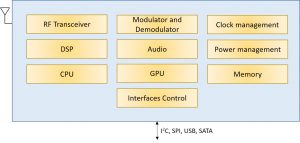
Figure 2 shows a diode string-triggered silicon-controlled rectifier (SCR), a commonly used electrostatic discharge (ESD) protection network for RF applications [5]. However, on a chip with many input/output (I/O) pads, only a fraction of the I/O pads that are RF/high speed require special ESD protection structures. It is not unusual for designers to have to check multiple specifications to ensure that all I/O pads have appropriate ESD protection structures present, and flag any that are non-compliant:
Only RF pads must have bipolar protection, with another bipolar transistor and a three diodes string connected between its base and ground. Other I/O pads use conventional ESD structures.
Gates connected to these RF pads must have a grounded silicide-block (SBLK) NMOS protection with a charged device model (CDM) resistor.
Output drivers connected to these RF pads must have resistor protection with a value between 40 and 60 ohms.
Grounded-gate NMOS protection between power and ground nets must have a minimum width of 400µm.
Figure 2: Diode string-triggered SCR for ESD protection of a RF I/O pad.
RF circuits are also very sensitive to parasitic elements and layout-dependent effects. To create a robust circuit that performs reliably over a broad range of operating conditions, both pre- and post-layout simulations are essential to verify that all parameters are in compliance with the design specification. This verification often requires many types of simulation analyses, including noise, linearity, power consumption, and stability. Either time domain or frequency domain simulation is used, depending on the type of circuit, type of analysis being performed, and the application. However, all of these simulations are compute-intensive operations that are both expensive (due to the hardware required) and time-consuming.
Because these circuits are so acutely sensitive to the effects of parasitics, circuit designers must work closely with the mask layout engineers to ensure that circuit implementation minimizes the impact of parasitics on the circuit operation. In particular, the insertion of fill patterns in the layout is crucial. While fill affects only capacitance at lower frequencies, it can significantly alter resistance and inductance when higher frequencies are used [2].
Performing device and ESD checks using visual inspection or traditional single-purpose verification tools is not only cumbersome and time-consuming, but also error-prone. SPICE tools require precise setup to catch subtle violations, a process that is susceptible to human error. At the same time, running dynamic simulations at the full-chip level to catch such violations is not always feasible, due to the sheer scale and complexity of modern SoC designs. While simulations are necessary to ensure the circuits achieve a baseline performance, both time and resources can be reduced by verifying device type, device properties, orientation, symmetry, and other critical design parameters before executing runtime simulations. Ensuring that a design is trending towards accuracy before running simulations ensures a quicker turn-around time (TAT) by minimizing both the number of simulation iterations and time spent in correction of post-simulation issues.
Automated verification solutions that can reliably and quickly verify that RF IC designs meet both technology and user constraints are vital to ensuring that design companies can deliver reliable products on schedule.
Design topology checking
Electronic design automation (EDA) verification tools are now available that are specifically designed to perform topological checking of circuits to address the complex verification requirements of RF IC designs. We’ll walk through the major verification strategies applicable to RF ICs, using the Calibre PERC reliability platform from Mentor, a Siemens business to demonstrate the automated verification capabilities available to RF IC designers.
Rule checks
Reliability verification tools can check a design against rule criteria provided by the foundry, as well as any specific requirements imposed by the design company. Designers can use foundry-supplied rules, or write their own simple rules as needed, to ensure that the correct type of circuit structures are used where required, and that appropriate connections are made with
these structures. For example, the Calibre PERC reliability platform can check multiple properties on devices (e.g., length, width, Vt type, etc.) and perform pattern matching to detect the presence and verify the correct construction of specific circuit structures.
These rule checks are not restricted to just the standard mainstream CMOS process. Foundries, designers, and computer-assisted design (CAD) engineers can define constraints and run rule checks for any device process, such as heterojunction bipolar transistors (HBTs) or RF silicon-on- insulators (RF-SOIs), both of which are commonly used in RF designs.
RF/Analog layout checking
Both the performance and reliability of RF designs are closely linked to the layout implementation. Once the physical layout of a RF design is complete, and circuit implementation is validated with layout vs. schematic (LVS) verification, many potential layout-dependent effects must be analyzed to avoid reliability and performance issues. While some of these effects can be caught during post-layout simulation, others won’t be seen until the design is on silicon, so finding and eliminating them during design verification is essential to chip and market success [6].
RF/analog mask layout designers typically follow various layout precautions that minimize the effects of crosstalk, mismatches, noise, etc. [7]. Some common techniques used by these designers include device symmetry, current orientation matching, dummy device insertions, common centroid and pitch between devices, and electrical parameters matching [6].
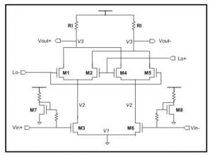
For example, differential circuits are commonly used in RF designs for low noise amplifiers (LNAs), mixers, power amplifiers, and charge pumps (Figure 3). In a fully differential circuit, any lack of symmetry between devices affects their ability to suppress the input common mode noise, introduces input referred offsets, and causes finite even order distortion [7]. These impacts make it critical to check for potential asymmetry in the circuits before tape-out.
Figure 3: A fully differential mixer [8].
To ameliorate the effect of the asymmetry inherent to the differential structure, layout designers add dummy devices on either side of the functional devices.
STI stress and WPE effects
Reliability is a key market consideration when designing RF circuits. Many RF products, such as the ones used in applications like aerospace, satellite communications, military, and defense, operate in harsh environments, and/or must operate for extended periods of time under stressful conditions, with time-to-failure criteria for these products stretching to, in some cases, multiple decades. Given these operating conditions and strict requirements, designers face stringent criteria for IC reliability when designing RF circuits.
Hence it is essential to take into account the impact of layout-dependent effects such as shallow trench isolation (STI) stress and well proximity effect (WPE), which can have severe consequences in terms of RF IC reliability and expected lifetime. Designers must understand their causes and check for susceptible layout structures when implementing RF circuits, and use proper layout techniques to mitigate the effect of these undesirable phenomena.
The effects of STI stress can be reduced by adding dummy devices and making the layout uniform and symmetrical [10].To minimize WPE, all devices that are expected to behave and age similarly should be matched together, and should have the exact same layout context, including spacing from the well edge. Verifying that these layout practices are followed using visual inspections or layout reviews is not ideal, as it is easy to miss violations. It is also difficult to ensure sufficient coverage, due to the size and complexity of today’s designs.
The Calibre PERC reliability platform provides consistent, automated detection of the most subtle errors in a layout implementation, such as device asymmetry and mismatches, missing dummy devices, or inaccuracy in a common centroid layout. As part of the Calibre PERC analog constraint check flow, designers define the checks they want to run, and select the devices on which the checks will be run. The Calibre PERC reliability platform runs the checks on the specified devices and displays the results in the Calibre RVE results viewing interface, highlighting the violations for easy viewing and fast correction.
RF/Analog layout fill insertion
To mitigate the thickness variation in copper interconnects resulting from the chemical mechanical planarization (CMP) process step in manufacturing, fill is inserted in the design. However, floating fill affects interconnect capacitance and alters the signal delay of interconnects [2]. If the fill impacts critical nets in the design, it can significantly reduce the performance of high speed and RF designs. As the frequency becomes higher, the effect on resistance and inductance become significant. Above 10GHz, the eddy current loss due to fill manifests as an increase in resistance [2], and can no longer be ignored.
On-chip spiral inductors are commonly used building blocks in RF circuits, but their electrical performance can also be affected by the presence of fill [11]. The fill shape size and the clearance of the fill from the signal wire of the inductor impacts the quality factor (Q-factor) and resonant frequency of the inductor.
Thus it is crucial to optimize the fill process, including consistent fill placement, sufficient
clearance of fill shapes from the critical nets, and determination of the optimum fill shape size to maximize performance, minimize the interconnect losses, achieve the desired Q-factor and resonant frequencies for inductors, and improve yield.
Design teams can optimize the fill generation process by placing fill consistently in the design, and preventing fill shapes from encroaching on areas that must be excluded from the fill process (Figure 4), using automated annotation and fill techniques. Designers can use the Calibre PERC reliability platform to automate the annotation of critical nets in their design prior to the fill generation step. The Calibre YieldEnhancer SmartFill fill process then automatically recognizes and honors any constraints imposed by exclude marker layers in the layout. This tool combination provides a tremendous advantage over traditional fill flows, where designers must either manually remove fill shapes around critical nets, or manually annotate these critical nets before the fill is added, both of which are slow, iterative, and error-prone processes.
Figure 4. a) Fill encroaching in the exclude regions near sensitive nets; b) Fill generated using combined Calibre PERC/Calibre YieldEnhancer flow that blocks fill from encroaching on the critical nets.
Adding Calibre Pattern Matching functionality to this combination can provide an automated orientation-aware fill flow, resulting in a consistent fill without any shifts in the fill pattern for elements such as inductors, gates, cells, etc. Designers capture unique configurations as patterns, fill each pattern in the most efficient and effective way, then save the filled shape as a new pattern. Whenever the original pattern is found in the design, it is then automatically filled to match the saved fill pattern, ensuring consistency throughout the layout, as shown in Figure 5 below [12].
Figure 5. Orientation-aware fill flow ensures symmetric and consistent fill pattern around the inductors.
Summary
RF IC designers face an increasing number of verification challenges due to technology scaling, growing integration with baseband and digital blocks, and the need to support multiple protocols, coupled with the push for more compact devices with lower power consumption, higher bandwidth, and throughput requirements. Relying on manual techniques and traditional simulation-based approaches is sub-optimal, resulting in increased tape-out times and potentially inferior quality designs, both of which can prove to be costly in today’s fast-moving and demanding markets. By leveraging the advanced functionality of EDA reliability verification tools to automate a variety of complex verification processes within every stage of the design from schematic and layout checking, and using an amalgamation of tool functionality to standardize and optimize post-layout fill insertion, RF IC designers can drastically reduce verification times while ensuring their designs will perform reliably in conformance with their design specifications over the lifetime of the products in which they are used.
Author
 Neel Natekar is a senior product engineer in the Design to Silicon division of Mentor, a Siemens business. He collaborates with R&D, field staff, and customers to define and implement new tools and functionalities that improve and expand automated design verification and optimization flows. Prior to joining Mentor, Neel worked as a design engineer at Qualcomm, focusing on power delivery solutions for their custom CPUs. He received a B.Eng. in Electronics and Telecommunications from the University of Mumbai, and an M.S. in Electrical Engineering, Circuits and Microsystems from the University of Michigan. Neel may be reached at neel_natekar@mentor.com.


