Article By : Maurizio Di Paolo Emilio

Diafilm TM220 is a chemical vapor deposition (CVD) diamond thermal grade that offers industrial users thermal conductivity in excess of 2200 W/mK.
Diafilm TM220 is a chemical vapor deposition (CVD) diamond thermal grade that offers industrial users thermal conductivity in excess of 2200 W/mK. Element Six (E6) launched this new solution in 2019 and, in an interview with EE Times Europe, Daniel Twitchen, chief technologist at E6, explained how over the last two years diamond has become a key enabler to many interesting applications, particularly in the thermal management of high power density radio frequency (RF) devices and application-specific integrated circuits (ASICs), as well as high-frequency resistive power management components. The introduction of this material to the market is in response to the ever-increasing demand for power that is pushing the limits of semiconductor thermal management.
Element Six’s Diafilm grades, spanning from 700 to 2200 W/mK, have applications in RF-based on gallium nitride (GaN) and monolithic microwave integrated circuits (MMICs) for phased array radar, space and satellite 5G base stations, and beyond. In addition, the success of terabit-speed optoelectronic networks for both metro and long-haul content delivery relies on highly efficient thermal management.
Diamond
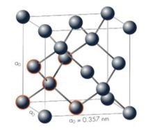
Diamond is characterized by its exceptional hardness, strength, optical and thermal properties. Natural diamond has an inherent scarcity and structural unpredictability that limit its use in engineering. Developments in synthesis have enabled the production of engineered synthetic diamonds that offer predictable properties and consistent performance; first in the 1950s using high pressure and high temperature and later in the 1980s using chemical vapor deposition (CVD) to produce the wafer scale diamond. The modern industrial world consumes about 800 tonnes of synthetic diamond, about 150 times the amount of natural diamond extracted as a gemstone.

Natural diamonds were first classified according to their optical properties. The most common type has an absorption edge of about 330 nm, and the minority with a value of about 220 nm. Over the years, this natural grading scheme has been extended, but in its broadest sense, it remains relevant to synthetic diamond.
The ever-increasing demand for power and bandwidth is pushing the boundaries of semiconductor thermal management. The move to higher frequencies is creating an opportunity for CVD diamond to rise as the ideal solution to enable more efficient thermal management.
Diamond growth by CVD process involves the preparation of a substrate by feeding a variable amount of various gases (carbon and hydrogen) into a growth chamber and then heating these gases, typically using microwave energy or a hot filament to temperatures higher than 2000°C. Its preparation involves choosing the appropriate material, its crystallographic orientation, cleaning it with diamond powder and optimizing the temperature of the substrate during growth to around 800°C through a series of tests.
During growth, the materials in the cavity are etched by the plasma and can be incorporated into the growing diamond. In particular, CVD diamond is often contaminated with silicon from both the cavity and the silica substrate.
The advantages of the CVD method include the possibility of synthesizing diamonds over large areas and especially on substrates with different shapes, with precise control over the chemical impurities and, therefore, the properties of the diamond produced, which is extremely useful in industrial applications since diamond is the hardest material known in nature and is the best thermal conductor, as it is extremely resistant to heat, radiation and acids. Diamond is also an excellent electrical insulator.
Diafilm TM220
The limitations of conventional thermal management solutions can put a tight bottleneck on components. This forces system designers in the aerospace, telecommunications and defence industries to make trade-offs between form factor, performance, and reliability.
Element Six’s TM220 is thermally isotropic, spreading heat as efficiently in a planar direction, with low density, chemical inertness and mechanical stability.
“Growing diamond using chemical vapor deposition means that, instead of growing small pieces of diamond, it’s now possible to reproducibly grow wafer-scale diamond with properties tailored for each application,” said Twitchen. “Pioneering work over the last 15 years has allowed the process development aimed at applications as diverse as diamond speakers for car audio systems to precision machining for smartphone manufacture, providing a great platform for the next generation of diamond-enabled markets. With increasing consumer demand for data and the adoption of new semiconductor materials driving significant increases in power densities, novel solutions are needed for dissipating heat. Leveraging diamond’s thermal conductivity, which can be 10 times higher than alternative solutions, brings a new and important solution to the semiconductor design book.”
The advent of new technologies and high-powered operating conditions in the automotive and transportation industries mean that new materials must be developed to meet stringent demands. The evolution and adoption of new technologies also puts pressure on consumer electronics companies and the tool manufacturers that support them. New 5G wireless technology, augmented and virtual reality and Internet of Things devices rely on new materials that are stronger and harder to machine.
CVD diamond solutions reduce thermal management bottlenecks and achieve lower operating temperatures.

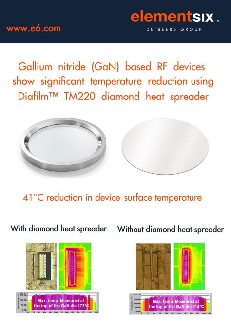
Twitchen pointed out that, with diamond, it is possible to distribute a significant amount of heat, spreading it over a much larger volume, thus reducing the junction temperature. Diamond has the potential to reduce the junction temperature by more than 30% compared to other solutions.
Heat control is a fundamental action for almost all semiconductor junctions. And at the same time, it comes up against the fact that we all want a smaller and longer battery. And typically, if devices get hotter, you lose efficiency and battery lifetime. “So if you can keep the devices cool, you get greater efficiency and better performance,” Twitchen said. “This might be particularly important in applications where pressure on size, weight and power are at a premium (SWaP) such as, for example, in satellites. Other thermal management solutions, such as aluminum nitride, have thermal conductivities around 200 W/mK. Diamond solutions with values 10 times higher than that are now a commercial reality, meaning that there is great potential to revolutionize many industrial markets.”
As with Diafilm’s other TM material grades, TM220 is thermally isotropic. It diffuses heat just as efficiently in a planar direction as it does through the material. Additional properties of Diafilm TM220 include dielectric permittivity, optical clarity, electrical insulation, low density, and chemical inertness.
Twitchen highlighted how Element Six has received positive feedback from the RF device packaging, X-ray generation and high-performance ASIC industries, which have all been early adopters of the TM220 grade. “Diafilm TM220 materials are available in standard thicknesses and can be manufactured to meet different customer requirements,” said Twitchen.
This article was originally published on EE Times Europe.
Maurizio Di Paolo Emilio holds a Ph.D. in Physics and is a telecommunication engineer and journalist. He has worked on various international projects in the field of gravitational wave research. He collaborates with research institutions to design data acquisition and control systems for space applications. He is the author of several books published by Springer, as well as numerous scientific and technical publications on electronics design.

