The advent of chips supporting millimeter-wave (mmWave) 5G signals is creating a new set of design and testing challenges.
Effects that could be ignored at lower frequencies are now important. Performing high-volume test of RF chips will require much more from automated test equipment (ATE) than is required for chips operating below 6 GHz.
“MmWave design is a pretty old thing,” said Yorgos Koutsoyannopoulos, vice president of R&D at Ansys. “What is different today is that we try to use those best practices on standard CMOS.”
Standard CMOS on a 5G technology should translate into high volumes – and that also is different. “MmWave is a relatively new phenomenon in production test,” said Tim Cleary, senior director of marketing, RF product group at FormFactor. “It started a couple of years ago in real volume. Auto radar was probably the first mmWave product that was really running at high volumes.”
While some of the challenges arise from the physics of high frequencies, others come from new capabilities like beamforming. In addition, test logistics must take into account whether to test devices over-the-air, as they would be used in a system, or through contact. Achieving an effective high-volume test process requires significant RF and mechanical expertise, which is in short supply.
“From an organizational point of view, successful design teams today bring two talents into the same team,” said Koutsoyannopolous. “One talent is people who have done millimeter wave design using III-V technologies like gallium arsenide or indium phosphide. The other is CMOS designers, who come from a low-frequency background.”
Not everything gets harder with mmWave design. Processing and inspections, assuming CMOS technology, remain the same. “We do not change how we inspect for mmWave,” said Ben Meihack, manager of inspection product marketing at Onto Innovation. “That is more on the packaging side.”
Packaging does get more complicated with antennas inside the package. But the most dramatic new challenge is testing.
High-volume silicon chips bring mmWave testing into the ATE world for the first time. Previous testing was done using benchtop setups, which can’t cope with the volumes that will be needed in the future. This has spurred significant development of high-frequency RF capabilities that can deliver the cost and throughput needed for economical production.
In an R&D lab, it’s all about making the most accurate measurement possible, whatever the cost or effort. High frequencies have been tested for years in low volume when characterizing silicon, and yet that’s being pushed further, as well.
“In the last year or two, the common frequency for characterizing cell silicon processes has been up to 110 GHz for 5G devices, because the transistor is modeled far beyond the operating frequency of the IC,” said Anthony Lord, director, RF segment business development at FormFactor. “That has now been pushed beyond 110 to 220 GHz, and even 330 GHz, as we get into devices working toward operating at millimeter waves up to 100 GHz.”
But for production testing, the goal is to make good-enough measurements at high speed, keeping throughput high. This means very different tradeoffs from what traditionally has been done at lower volumes.
“The production guys are not interested in the best measurement they can get,” said Cleary. “Rather, they need the least accuracy they can get away with.”
5G changes the game
The exact bands and numbers of bands vary by region, but they tend to be in the 26, 40 and 50+ GHz ranges. Each band needs a front-end and an antenna array.
While radar chips may have from one to three or four lines, 5G chips will have more like 30 lines. “At the volumes that a 5G cell phone are likely to have, they want to be testing four or eight at a time,” said Cleary. “So now we’re talking about upwards of 200 mmWave lines, where before they weren’t testing any.”
And there will be many mmWave chips. “A 5G mmWave handset will have 2 to 3 mmWave devices for every traditional sub-6 GHz transceiver,” noted Stephen Pruitt, wireless segment manager at Teradyne.
Fortunately, for the moment, mmWave implementations for 5G aren’t ready for deployment. “In the world of 5G, it’s beyond prototype, but it’s limited production,” said Steve Sergeant, CEO of Marvin Test Solutions.
MmWave frequencies make design and testing more difficult than RF testing below 6 GHz. The rules change at frequencies above around 26 GHz. While there is no hard cutoff for this transition, the gaps between bands place 6 GHz firmly below the transition, and 28 GHz firmly above.
“Signal path losses and impedance mismatches are amplified at these higher frequencies and can greatly impact signal fidelity,” said Pruitt. “Where interface boards at 6 GHz will have less than 3 to 5 dB of loss total between cable, PCB, and contactor interface, an interface board designed to function at 40 GHz will see 2X to 4X more loss for the same signal chain.”
This has implications for the test setup. “It becomes more difficult to calibrate accurately to the tip of the probe, and the calibration drifts faster,” said Lord, citing one example.
Making matters more challenging for chip and test-fixture design, every piece of metal along a signal path must be treated like a transmission line, both on- and off-chip. Even for aggressive process nodes, on-chip metal lines will have lengths in the micron range — as high as 100 microns. A 30 GHz signal will have a wavelength around 10 mm, which is too close to the metal lengths to ignore the transmission line effects. This affects design as well as test.
“At those high frequencies, we have electromagnetic effects that affect the performance substantially,” said Koutsoyannopoulos. “So, unless you take these effects into account very carefully, you cannot really simulate the performance of these designs.”
“There are no parasitic components anymore,” added Anand Raman, senior director of applications engineering at Ansys. “Everything is a mindfully designed component. Some of them are active components and the rest are passive components, and they’re all talking to each other at all times.”
Failure to verify all of the frequency effects on the lines could result in inaccurate current calculations. Moreover, it turns the simple act of connecting components into a complex analysis.
Antennas in the package
At these dimensions, antennas can be co-packaged with the chip – so-called “antenna-in-package,” or “AIP.” Dipole antennas don’t work well, so patch antennas are used in arrays for beamforming. This requires codesign of the chip, antenna, and package to fully comprehend all of the high-frequency effects.
“At mmWave frequencies, the antennas are much smaller and more numerous,” said Pruitt. “This allows chip and module manufacturers to include antennas in the device packaging. It is this packaging that creates a new set of challenges when looking to source and measure signals to the DUT.”
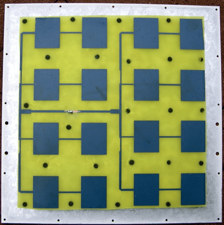
Fig. 1: An array of patch antennas. Source: Serge Nueffer at French Wikipedia, transferred to Commons by Bloody-libu using CommonsHelper., CC BY-SA 3.0
And there are likely to be many antenna elements. “You might have 16 elements that are working at 28 GHz and another 16 elements that are working at 40 GHz,” noted Cleary.
To contact or not to contact
One of the fundamental questions to answer when testing a wireless technology is whether or not to test it wirelessly. This comes down to a debate between contact testing and over-the-air (OTA) testing, and views differ.
Contact testing relies on probes touching pads and making measurements directly. It short-circuits the antenna and looks directly at the signals being presented to the antenna. It’s much easier to do, and losses are much lower. But it doesn’t include package and antenna effects in a finished product.
“You’re not going to get away with anything better than real contact for highly accurate dependence modeling and characterization in the R&D world,” said Lord.
For wafer sort, contact testing means touching the pads, and this is by far the predominant method at the wafer level. There’s no practical way to connect an antenna, and there’s no package yet to worry about, so that’s the easiest, most cost-effective way to get dies tested before the wafer is singulated.
At final test, contact testing means contacting the balls of the package. There are typically balls under the antenna – used only for testing – to allow for contact testing of the chip itself. But this leaves out important behaviors.
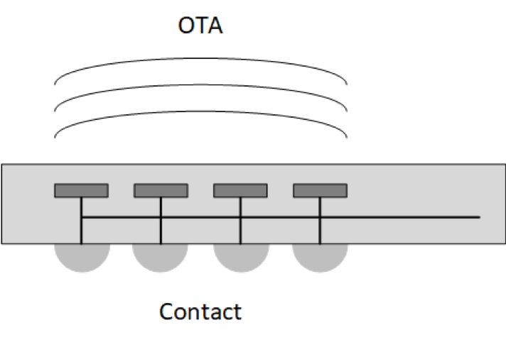
Fig. 2: Contact to the internal patch antenna elements typically is provided to external balls, as shown in simplified form. Contact testing can be performed by accessing balls; OTA testing can be performed using receiver patch antennas outside the package. The balls serve no operational purpose – they’re there for test access only. Source: Bryon Moyer/Semiconductor Engineering
For a packaged part, OTA testing gives a much more realistic view of how the device will perform in a real system. “For module testing, the challenge is how to measure the device without touching it,” said Pruitt. “Any contact with the antennas using a conductive material will change its characteristic impedance and impact performance. In this situation, radiated testing is the only method for testing these devices.”
But OTA testing is difficult, and at present it’s expensive to achieve. The losses are much higher and must be coped with, so some consider contact testing to be better. But others are requesting OTA testing simply because it is more complete.
Having a chip radiate a signal with multiple antennas to pick up the result and analyze it in the tester brings mechanical and field challenges that are still being worked out. The solutions that have been found to work are expensive to implement – especially for high volumes.
One of the main challenges for OTA testing relates to how far the antenna should be from the transmitter. Fields operate differently in the so-called near field and far field. In actual use, receiving antennas will be well into the far field, so that’s the most realistic way to test.
Far-field testing is difficult. “There’s always a challenge to test far-field, especially at the lower frequency range [sub-6 Hz], where you need huge distances,” said Adrian Kwan, business development manager at Advantest. But even with mmWave frequencies, far-field testing would require an antenna on the order of 90 mm away.
That’s still impractical for a production tester. “In the ATE space, it’s hard to deploy far-field for high-volume multi-site production,” said Kwan.
What’s promising is there are established ways of taking near-field measurements and correlating them to their far-field equivalents, according to Kwan. This can bring the spacing down to under 9 mm.
Doing all of this at volume, however, involves every piece of the testing infrastructure. “As far as interference is concerned, mechanical socket design presents a lot of challenges,” noted Kwan.
They’ve designed a socket that can handle both kinds of test. “It’s very similar to a regular socket, except that it has built-in patch antennas,” he said. “It can test all your digital and DC stuff on the package balls, but it also does the OTA with the patch antennas.”
An alternative to having patch antennas in the near field is to do self-radiation. “In this case, the socket acts as a reflector and the device antennas are effectively looped back on themselves,” said Pruitt. “While this allows for simpler tester configurations, it prohibits key tests like transmit compression, EIRP, and receive sensitivity.”
Dealing with beamforming and loopback
Beamforming, which uses phase differences in elements of an antenna array to steer a beam in a particular direction, brings its own challenges to the test program. Beamforming makes for more efficient energy usage, because the signal for a given 5G subscriber is aimed directly at the subscriber rather than being broadcast in all directions, which is what we have today. Most of that broadcast signal energy is wasted.
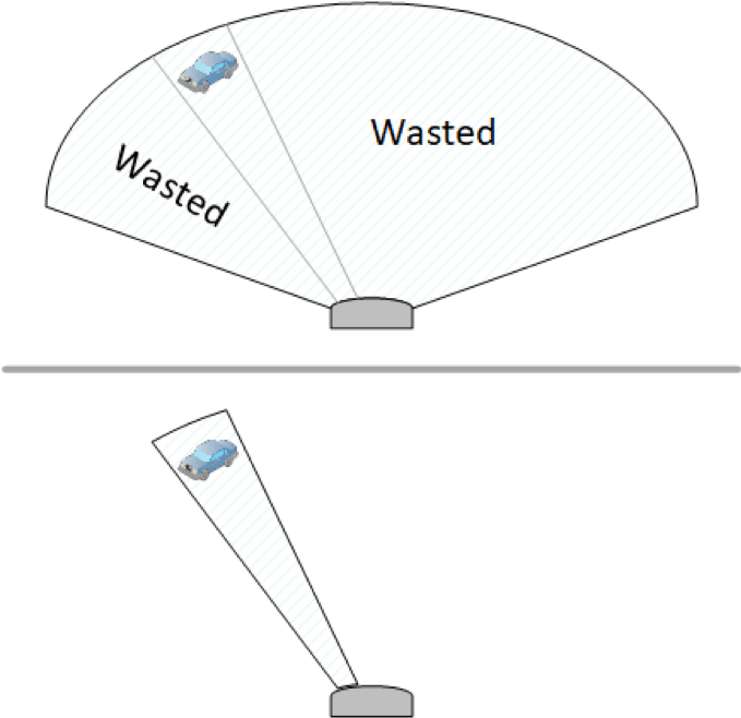
Fig. 3: The top portion shows the typical situation today, where a signal is broadcast with most of that signal being wasted. Beamforming focuses energy only on the desired target, as shown on the bottom, and the remainder of that wasted energy is now saved. Source: Bryon Moyer/Semiconductor Engineering
“Fast beam steering is an essential characteristic of these devices, and it is accomplished by storing pre-defined states in the device registers, which are then called as required, thus greatly improving the device’s response time,” said Joe Semancik, director of marketing at Marvin Test Solutions.
But this capability needs to be tested. “While we still see the traditional radio tests (ie. gain, phase noise, modulation quality, etc) in these mmWave devices, the inclusion of beamformers requires the ATE to test things like absolute and relative phase/gain on the different antenna element connections,” said Pruitt. “Having the ability to calibrate the phase and amplitude of the ATE hardware and provide signal de-embedding to the DUT is critical to achieving quality performance testing.”
With contact testing, this can be done by measuring the phase relationships between antenna elements to ensure that they’re working properly. For a packaged part, this is done by accessing the balls under the antenna.
For OTA testing, multiple receiver antenna patches are needed. One can be used as the reference, with the others then measured relative to the first one. Testing can then proceed from 0° to 180° phase differentials.
One alternative option to OTA testing is loopback, a familiar concept for any transceiver design. It takes a single transceiver, transmits a signal, and then routes it back to the receiver within that same transceiver. It’s easy to do with wire or switched connections for lower frequencies, but it’s much more difficult at mmWave frequencies.
A benefit of internal loopback testing is to bypass the mechanical test setup. “There’s no environmental consideration. There’s no tester effects,” explained Kwan. “So this is as good as golden-device testing, where a good transceiver transmits a signal, and then the same transceiver measures it.”
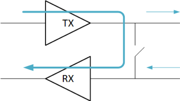
Fig. 4: During operation, the transmitter (TX) sends a signal to the antenna, and the receiver (RX) brings a signal from the antenna. For testing purposes, loopback routes the transmitted signal directly back into the receiver. Source: Bryon Moyer/Semiconductor Engineering
Loopback at these frequencies isn’t easy, however. “Not many of the fabless transceiver players are able to deploy loopback,” said Kwan. And those companies that can consider those circuits to be critical IP.
Implementing loopback on the DUT board is particularly difficult. “One millimeter of transmission line completely changes your spectrum,” said Kwan. “So you need to be really careful doing loopback through the load board.”
Even when successful, however, loopback testing is sub-optimal. For one thing, it doesn’t take the full package and antenna into account. In addition, golden-device testing is subject to errors, according to Kwan. Customers are much more interested in having instruments take an objective measurement rather than using relative measurements.
“Right now, a lot of customers are either doing loopback testing, or they’re testing the antenna separately,” said Kwan. “In the future, they will need to be able to test a complete AIP module in high-volume production.”
Improving throughput
Multi-site testing is a must-have for lowering cost and improving throughput. Such testing is straightforward when doing contact testing. But when doing OTA final test on a packaged part, it means that multiple chips need to be concurrently tested without interfering with each other. Solutions have been found for this, with Advantest claiming to have a working eight-site solution.
Parallel testing may also be possible across bands. “If the system is capable of handling multiple frequencies at different ports, you could test the sub-GHz and the mmWave frequencies at the same time,” said Kwan. Each band has its own frontend, so testing multiple bands would require being able to drive multiple independent RF signals concurrently.
It’s different for multiple channels within a band. Each channel is 100 MHz wide, but they all use the same front-end. That means that the tester can mix the signals of different channels into the same front-end and run all channels with full duplex simultaneously, which is similar to what would happen in a real system.
For beamforming, it’s also possible to do independent tests on different channels at the same time. One can drive one channel to beam to the left while another beams to the right. It’s then up to the receiver to split the results into the independent channels for verification.
Chips also may have more than RF circuitry on them. There is likely to be digital circuitry on-board at the same time — at least for controlling the RF module. That digital circuitry can be tested in the same insertion as the RF, so separate testers or insertions aren’t necessary.
This is possible due partly to the fact that when looking at all of the chips of all kinds being tested, a small minority of them will need mmWave test.
“If you’re going to bring on one of dozens of chips that needs 200 mmWave lines, and all the rest of the chips that you have running through your factory get by with less than 20, then are you really going to build a dedicated tester that has the capability for all that stuff, or are you going to try to figure out some other way of doing it?” asked Cleary. “What customers want is to have a tester that has the core capability needed for the majority of the chips that they plan on testing and then put the extensions to that tester on the probe card to cover the entire portfolio.”
While saving costs in the tester, it makes for more expensive and complex load boards, which will need components like RF switches and up- and down-converters.
Economics usually dictate fewer insertions, but that may not always be the case. “One tradeoff a customer might see is all the non-RF tests burdened with the additional costs associated with mmWave tests,” noted Pruitt. “In a couple of cases, we have seen customers look at multiple insertions to separate some non-RF tests (mostly DC & scan) from the RF tests.”
The last big barrier: economics
Many technical issues have been solved for mmWave testing. While other issues remain, the big challenge is cost. Especially for OTA testing, mmWave testing is an expensive proposition, and that could slow its adoption.
“Testing millimeter-wave frequencies is not inexpensive,” said Cleary. “It’s not for the faint of wallet.”
The good news is that much of this development can be carried forward for the next generations. “6G is probably a decade down the road, but they are discussing what bands could be used in the future,” noted Kwan. Those frequencies seem to be moving in only one direction — up.
But that doesn’t mean that there won’t be more work then. “They’re talking about operating frequencies of up to 200 GHz,” said Lord. “If you get to those frequencies, it becomes a lot more complicated because there’s no single connector to cover that broad range.”
More creative engineering will be required to develop economic solutions for the next generation.
